Bus Pirate 6 · Volume 2
Bus Pirate 6 Volume 2 — Hardware: RP2350B, the Look-Behind Buffer, and the Per-Pin Level Translators
Schematic-grade walk — MCU, 74LVC1T45 per-pin level shift, 74LVC8T245 logic-analyzer tap, PPSU, ADC mux, NAND, LCD, RGB indicators
2.1 About this volume
This is the schematic-grade hardware walk for the Bus Pirate 6 REV2. Where Volume 1 introduced the platform and explained where the BP6 sits in the bench, this volume goes inside the case and follows every signal from the probe pins back to the RP2350B. Read this when you’re going to design a custom plank, modify the hardware, debug a level-translator-related symptom, or need to know exactly what the firmware can ask the silicon to do.
The canonical hardware-doc is docs.buspirate.com/docs/hardware/bp6rev2/hardware/; the canonical firmware source-of-truth is the boards/ and platform/ directories of DangerousPrototypes/BusPirate5-firmware. Where the two disagree, the firmware wins — silkscreen sometimes lags reality by one PCB rev.
2.2 RP2350B SoC
The Bus Pirate 6 is built around the Raspberry Pi RP2350B — the 80-pin QFN variant of the RP2350 microcontroller (vs the 60-pin QFN-60 RP2350A used on the Bus Pirate 5XL, and the older RP2040 used on BP5 REV8 / REV10).
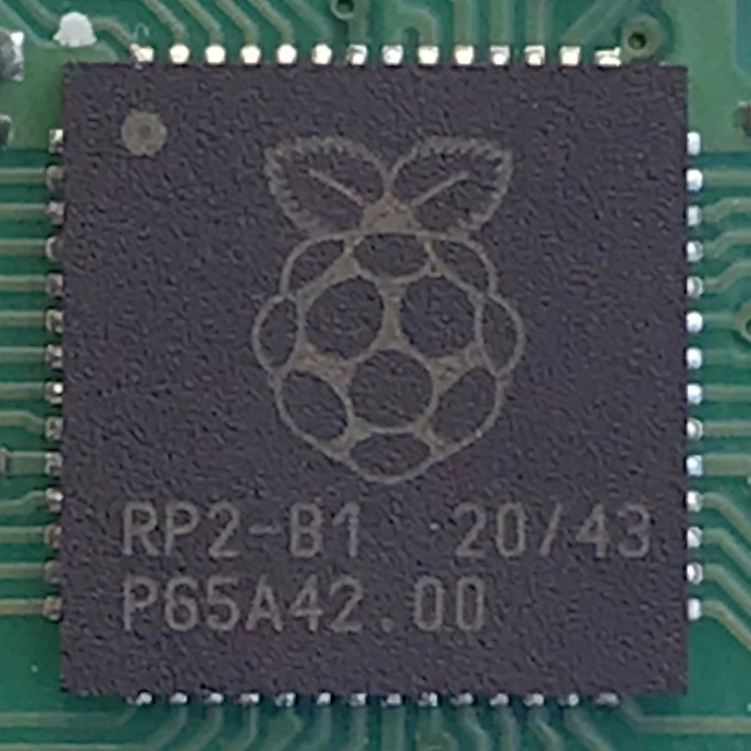
Figure 2.1 — File:RP2040 Microcontroller (cropped) RP2040-B1.jpg by Thomas Glau. License: CC BY-SA 4.0. Via Wikimedia Commons.
2.2.1 Two cores of four — the ARM/RISC-V choice
The RP2350 has two pairs of CPU cores in the same package:
- 2× ARM Cortex-M33 at 150 MHz (the “main” cores, with FPU + DSP extensions + TrustZone)
- 2× RISC-V Hazard3 at 150 MHz (open-source RISC-V, no FPU, simpler microarchitecture)
Only one pair runs at a time. The architecture choice is made at boot — Raspberry Pi’s picotool writes a flag in the start-of-flash header that tells the boot ROM which pair to spin up. You cannot mix ARM-M33 and RISC-V Hazard3 in the same firmware build; you pick one. The Bus Pirate 6 firmware ships ARM-M33 by default in the bus_pirate6_rev2.uf2 build target. A community RISC-V build exists but is experimental — wider firmware support is in the Pico SDK rather than the Bus Pirate firmware tree per se.
Practical consequence: the BP6 has two M33 cores actually doing work, not four. Bus Pirate firmware is fundamentally single-core-leaning (the syntax runner is a serial-state-machine; PIO offloads do the heavy I/O lifting), so the second M33 sees light use — mostly USB-CDC servicing and the display update path.
2.2.2 Memory, PIO, and the FPU
Table 1 — 2.2 Memory, PIO, and the FPU
| Resource | RP2040 | RP2350A / B |
|---|---|---|
| SRAM | 264 KB | 520 KB |
| Internal flash | none (uses external QSPI flash) | none (same external-QSPI architecture) |
| PIO blocks | 2 | 3 |
| PIO state machines total | 8 (4 per block) | 12 (4 per block) |
| Hardware FPU | no | yes (ARM-M33 FPv5-SP, single-precision) |
| Cryptographic accelerators | no | AES, SHA-256, true RNG |
| TrustZone | no | yes (M33 secure/non-secure split) |
For the Bus Pirate 6, the practical wins over the RP2040 of the BP5 are:
- Twice the SRAM — the firmware’s on-board file buffers, syntax bytecode scratch space, capture buffers, and on-screen frame buffers all grow without contention.
- One more PIO block / four more state machines — enough headroom for the look-behind logic-analyzer capture (§ 5) to run on its own block independent of the active mode driver.
- Hardware FPU — irrelevant for most protocol work, but the BP6’s voltage-rendering and current-display paths use floating-point conversion that was integer-emulated on the BP5.
- The cryptographic accelerators are unused by current firmware but available for future smart-card and bus-encryption work.
2.2.3 The 18 extra GPIOs — why BP6 exists
The RP2350B has 18 more GPIOs than the RP2350A — 48 vs 30. This is the entire reason the Bus Pirate 6 exists as a distinct product from the 5XL: the 18 extra GPIOs let the design drop the 74HC595 shift registers that BP5 / BP5XL needed for status LEDs and indicator routing, and they enable the parallel-tap 74LVC8T245 look-behind buffer (§ 5) which is the BP6’s distinguishing feature.
GPIO allocation on the BP6 REV2 (approximate, see firmware boards/bus_pirate6_rev2.h for the canonical map):
Table 2 — GPIO allocation on the BP6 REV2 (approximate, see firmware boards/buspirate6rev2.h for the canonical map)
| GPIO range | Purpose |
|---|---|
| 8 × dedicated for IO0–IO7 drive | per-pin 74LVC1T45 control |
| 8 × dedicated for IO0–IO7 sample | 74LVC8T245 look-behind buffer outputs |
| 4–5 × dedicated for the ST7789V LCD SPI | TFT control, DC, RST, BLK |
| 2 × for the on-board SPI NAND | additional SPI bus |
| 1 × WS2812 / SK6812 data | 18-LED chain |
| 6+ × buttons, USB-C status, debug-misc | reset, BOOTSEL, button-press, etc. |
| 16 × for CD4067 mux address + analog | per-pin voltage measurement |
That comfortably fits in 48 GPIOs with headroom. On a 30-pin RP2350A you’d need shift registers to multiplex many of these — exactly what BP5 / BP5XL did.
2.2.4 RP2350 errata E9 — the pulldown latch
The RP2350 silicon launched (Aug 2024) with a documented hardware errata E9: the internal GPIO pulldowns latch as bus-hold elements under certain conditions. Symptoms: a pulldown that should slowly bias an unconnected pin to GND instead “remembers” the last logic level applied, behaving more like a weak bus-keeper.
Mitigation on the BP6 board: 100 kΩ external pulldown resistors at each IO pin, populated from the factory. The firmware also avoids relying on the internal pulldowns for any timing-critical pin discipline.
Practical consequence for the user: most workflows don’t see this — the external pulldown is strong enough for any normal hold-low behavior. The one place errata E9 still surfaces is JTAG/SWD pin-find on targets that expect strong pulldowns: some chips’ SWDIO float-detect logic looks for a stronger ground bias than the BP6’s 100 kΩ provides. If bluetag (Vol 7) returns “no SWD found” on a target you’re sure has one, try wiring an external 4.7-10 kΩ pulldown to GND on the suspect SWDIO pin and re-scanning.
The errata is silicon-side; Raspberry Pi has not yet announced a silicon respin. The BP6 hardware-workaround is the long-term solution.
2.3 Power domain
2.3.1 USB-C input
A standard 5 V USB-C receptacle on the side of the case. The BP6 negotiates as a USB 2.0 high-speed device (480 Mbit/s) — no USB Power Delivery handshake, no USB 3.x. The host supplies the full 5 V / ~500 mA budget the device might draw at peak (display + LED chain + PSU output at full current + RP2350B at full clock).
USB-C wiring on the BP6 follows the standard 2-resistor CC1/CC2 pulldown topology so any USB-C cable plugs in either orientation. There’s no DisplayPort alt-mode, no audio accessory mode, and no power-output mode — the BP6 is always a USB-C device, never a host.
The schematic uses an ESD diode array between VBUS and GND for the USB-C connector to protect downstream silicon from cable-insertion ESD events.
2.3.2 The external 1.1 V LDO (not the on-chip SMPS)
The RP2350 has an integrated switching-mode power supply (SMPS) that can generate the chip’s internal 1.1 V core voltage directly from 5 V. The BP6 design chooses not to use it — instead, an external linear regulator (LDO) generates the 1.1 V rail.
Rationale: the on-chip SMPS is cheap silicon but produces switching noise that contaminates the per-pin ADC measurement path (§ 7) and the PPSU current-sense readings (§ 6). At a few cents of BOM cost, an external LDO eliminates that noise floor entirely. This is a recurring theme in the BP6 design — current-sense and voltage measurement are protected from on-chip noise by extra external silicon, because the target user is going to care about millivolt-level differences.
2.3.3 3.3 V rail and protection
A separate 5 V → 3.3 V LDO (typical AMS1117-3.3 or equivalent) feeds the RP2350B’s IOVDD pins, the 74LVC1T45 chain, the 74LVC8T245 look-behind buffer, and the ST7789V LCD controller. The 1.1 V from § 3.2 feeds only the RP2350B’s VDD core domain.
Polyfuses or reverse-polarity protection on the input rail (USB-C VBUS is normally guaranteed-correct polarity, but the design plays safe for accidental external power injection on probe pins back through the per-pin buffers).
2.4 Per-pin level translators — 74LVC1T45 ×8
This is the heart of what makes the Bus Pirate flexible across target voltages. Every one of IO0 through IO7 has its own dedicated 74LVC1T45 chip — eight separate level translators, not one octal device.
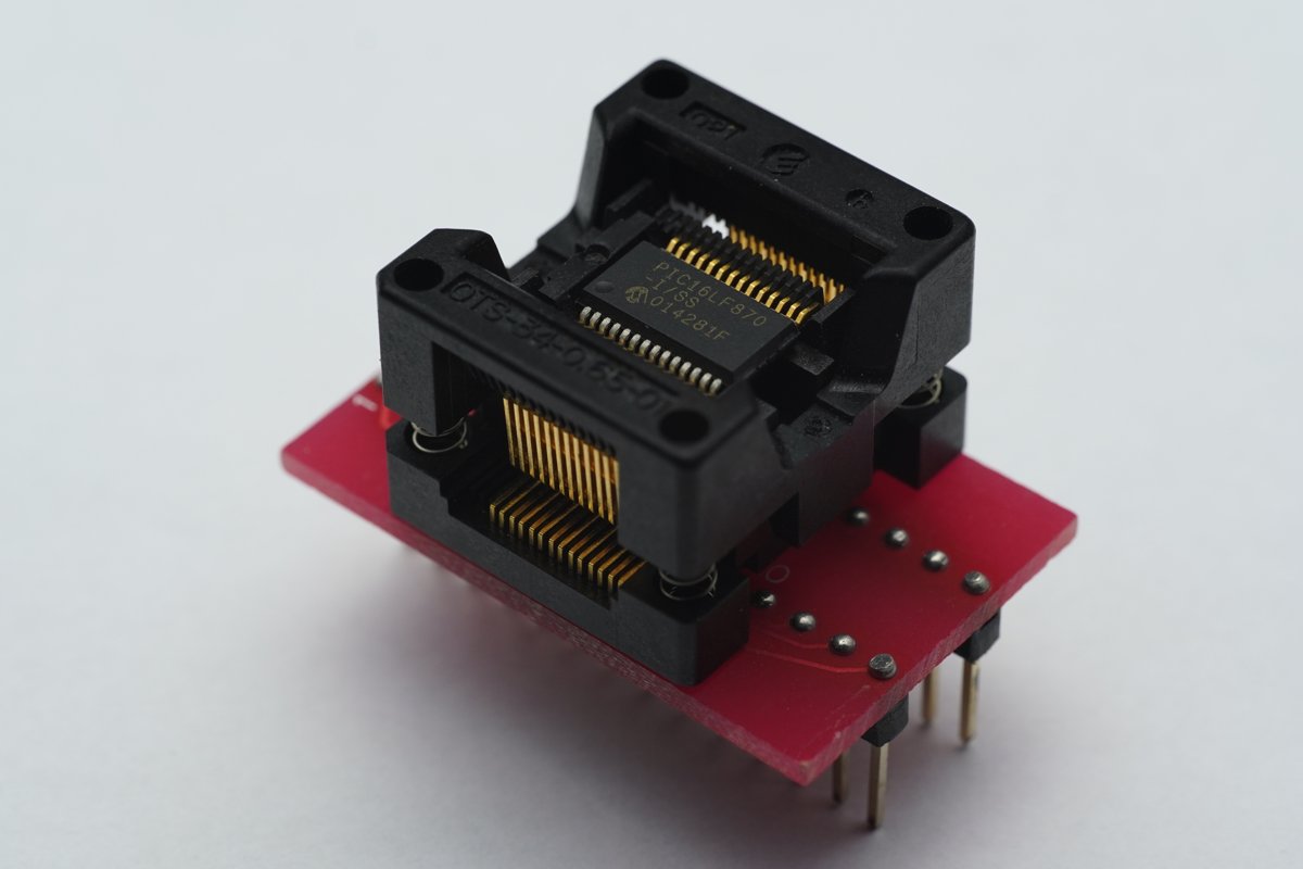
Figure 2.2 — File:PIC16LF870 in SOIC Socket.jpg. License: CC BY-SA 4.0. Via Wikimedia Commons.
2.4.1 What the 1T45 is and why it’s used here
The 74LVC1T45 is Texas Instruments’ single-bit dual-supply bidirectional level translator. Two supplies — VCCA (the “A” side) and VCCB (the “B” side) — and a single DIR input controls direction. The supply rails are independent: VCCA can be 1.65–5.5 V and VCCB independently 1.2–5.5 V, with no required ordering between them. The chip auto-handles whatever logic-level mismatch sits between its A and B sides.
For the Bus Pirate 6, VCCA is fixed at 3.3 V (the RP2350B IO domain) and VCCB tracks whatever target voltage the PSU is set to — or, when the PSU is off, whatever voltage the target itself is pushing onto the probe pin. The target side floats with whatever the bus is doing; the RP2350B side always sees clean 3.3 V logic.
Why this matters in practice: the BP6 can talk to a 1.8 V target (modern smartphone SoC debug), a 3.3 V target (Raspberry Pi GPIO, most modern flash), a 5 V target (Arduino / classic TTL), or anything in between, with no jumpers, no level-shifter board, and no manual reconfiguration. The PSU command (W 1.8 for 1.8 V output, or W 5 for 5 V) sets the PSU output AND the VCCB of the level translators — they’re the same rail.
2.4.2 The per-pin chain: PFET pull-up, series R, the buffer, the pad
Walking from the RP2350B side outward to the probe pin, the per-pin chain looks like:
RP2350B GPIO (3.3 V logic)
    ↓
74LVC1T45 A-side (VCCA = 3.3 V)
    ↓ ↑ (DIR controlled by another RP2350B GPIO)
74LVC1T45 B-side (VCCB = PSU voltage, 1.0–5.0 V)
    ↓
SI2301 PFET (pull-up gate; source = VCCB; drain → 10 kΩ → pin)
    ↓
120 Ω series resistor (short-circuit protection)
    ↓
Probe pin (IO0–IO7 at the 10-pin TJC8A header)
A few details that matter:
- The 120 Ω series resistor is the short-circuit safety margin. If a probe pin accidentally touches a power rail it shouldn’t, the 1T45 driving the line into a contradiction sees a current-limiting series impedance. At 5 V into 120 Ω that’s a worst-case 41 mA — well within the 1T45’s per-pin output rating (32 mA continuous, higher transient).
- The 10 kΩ pull-up, when enabled, ties the probe pin weakly to VCCB. The PFET gates whether it’s connected at all.
- Per-pin voltage measurement (via the CD4067 mux, § 7) taps the probe pin between the 120 Ω resistor and the 1T45 B-side output. So the BP6 always sees what the actual probe pin sees, not what the 1T45 thinks it’s driving.
2.4.3 SI2301 PFET pull-up gating
The SI2301 is a Vishay P-channel MOSFET in SOT-23. Vgs(th) is around 0.85 V — it turns on solidly with the RP2350B’s 3.3 V GPIO control line pulling its gate low. When the gate is pulled high (matching VCCB), the FET is off and the pull-up is disconnected.
Why use a PFET gate instead of just driving the pull-up from a GPIO directly? Two reasons:
- Variable VCCB. The pull-up needs to bias the target pin to whatever VCCB is — 1.8 V, 3.3 V, 5 V. A direct GPIO drive would always pull up to 3.3 V regardless of target.
- Disabling the pull-up reliably. With a PFET gate, when the gate is high, the source-drain path is high-impedance — the pull-up resistor is electrically disconnected from VCCB. There’s no leakage path.
The 10 kΩ pull-up resistor is the conventional I²C value. For 1-Wire and 3-Wire (Microwire) you also want it. For SPI / UART / JTAG / smart-card, you turn it off — the bus has its own driving silicon and the pull-up would just waste power.
Pull-up state is per-pin: you can have IO0 pulled up for I²C SDA, IO1 pulled up for I²C SCL, and IO2 not pulled up because it’s a level translator’s direction output you’re tapping. Each PFET has its own gating GPIO.
2.4.4 Why 8 separate translators instead of one octal
A 74LVC8T245 octal level translator would shift 8 lines in one chip — saving 7 ICs and a bunch of PCB area. The BP6 doesn’t use one for the probe pins because the direction has to be controllable per-pin, not per-group:
- IO0 might be SDA (input mostly), IO1 might be SCL (always driven), IO2 might be MOSI (always driven by BP), IO3 might be MISO (always driven by target).
- An octal 8T245 has a single DIR pin for all 8 bits — they’re all “BP→target” or all “target→BP” at once. That’s useless for a multi-protocol bus where different lines have different direction at the same instant.
The 1T45 has per-chip DIR — and with 8 separate 1T45s, you get 8 independent direction controls. The cost is ~70-80 cents extra in BOM, more board area, and 8× the DIR-pin GPIO usage (precisely why the BP6 wanted 48 GPIO — it has 8 to spare for this).
The other 74LVC8T245 on the board — the look-behind buffer, § 5 — does use one octal chip because it has only one direction (always “bus → RP2350B”). That’s an exception, not the rule.
2.5 The look-behind buffer (74LVC8T245) — BP6’s defining feature
This is the one piece of BP6 hardware that doesn’t exist on the BP5 or BP5XL. Everything else in the BP6 design is a refinement; this is a new capability.
2.5.1 Schematic — how the 8T245 taps the bus
The 74LVC8T245 is the octal sibling of the 1T45 from § 4 — 8 bits of bidirectional level translation in a single TSSOP-24 package, with one DIR pin shared across all 8 channels. On the BP6, the 8T245 sits physically in parallel with the per-pin 1T45 chain: each of its B-side inputs is wired to the same probe-pin net the corresponding 1T45 drives.
                                                  +---- 74LVC1T45 (per-pin driver)
                                                  |        DIR ← RP2350B
                                                  |        A ← RP2350B GPIO (drive)
                                                  |        B → probe pin
Probe pin IO0 ────────────────────────────────────┤
                                                  |
                                                  +---- 74LVC8T245 (look-behind)
                                                          DIR = always B→A (target→RP)
                                                          B ← probe pin (parallel tap)
                                                          A → RP2350B "sample" GPIO
The 8T245’s DIR pin is hard-wired to “B → A” — always sampling, never driving. Its A-side outputs land on 8 dedicated RP2350B GPIOs that the firmware uses purely for sampling.
This is the key trick: the 8T245’s high-impedance sample input doesn’t load the probe pin, so the 1T45 can drive the pin normally while the 8T245 watches. Both buffers operate from the same VCCB rail, so they see the same target voltage; both translate to 3.3 V for the RP2350B side.
2.5.2 The 8 dedicated RP2350B GPIOs that read the buffer
The 8T245’s A-side outputs go to 8 GPIOs that don’t appear in the BP5 / BP5XL design — these are GPIOs that only exist on the RP2350B. The BP5XL with RP2350A doesn’t have enough GPIOs to wire up a parallel-sample buffer; the BP6 with RP2350B does.
The 8 sample GPIOs are mapped contiguously where possible so a single PIO state machine can read all 8 bits in parallel with a 1-cycle GPIO read. That’s the architectural choice that makes the look-behind capture fast enough to be useful.
2.5.3 The PIO sampling architecture
The BP6 firmware reserves one PIO state machine on PIO block 2 (the third PIO, exclusive to RP2350) for the look-behind capture. The SM program is short:
.program look_behind_sample
    in pins, 8        ; read 8 sample-GPIO bits
    push noblock      ; push to the RX FIFO; drop if full
That’s it. The state machine free-runs at the PIO clock divider’s selected rate, reading IO0–IO7 in parallel and pushing each 8-bit sample to the FIFO. A DMA channel drains the FIFO into a circular buffer in SRAM. When the user runs a capture command (or when PulseView attaches over the BPIO2 protocol), the host pulls samples from the buffer in real time.
The mode driver (SPI, I²C, UART, etc.) is completely unaware that this is happening — it drives the bus exactly as it would on a BP5. The look-behind capture runs in parallel as an independent PIO state machine on independent GPIOs.
2.5.4 Bandwidth and what sample rates are achievable
The PIO clock can run as fast as the system clock — 150 MHz on the RP2350. With the simple in pins, 8 / push noblock program at 1 cycle per loop, the theoretical sample rate is 150 Msps.
In practice, the sustainable rate is limited by:
- DMA bandwidth from PIO RX FIFO to SRAM — fine for the rate above.
- USB-CDC out rate to host — the BP6 enumerates as a USB 2.0 full-speed device (12 Mbit/s, ~1.5 MByte/s effective). At 150 Msps × 1 byte/sample, that’s 150 MB/s being generated and 1.5 MB/s being drained. The circular buffer fills in 150/1.5 ≈ 100 µs of capture before sample loss starts.
- PulseView’s expected timing — PulseView’s BPIO2 driver runs at sub-MHz sample rates for steady-state work; 100 Msps capture is a “burst then drain” workflow.
The practical sweet spot: 40-100 Msps for short bursts (a few hundred ms of capture), 1-10 Msps for sustained capture (the host can drain the buffer at this rate without overflow). For a SPI flash dump session that runs at ~10-30 MHz SPI clock, capturing at 40-50 Msps gives 4-5× oversampling — more than enough to recover clock edges and verify data.
2.5.5 Why BP5/5XL can’t do this and BP6 can
The BP5 and BP5XL bit-bang the same pin they drive. The protocol drivers in firmware time-slice between driving the bus and sampling it on the same GPIO. There’s no “parallel” — every sample point is interleaved with a drive operation.
For most workflows that’s fine: a SPI master drives MOSI and reads MISO; it never reads MOSI back after driving it. But for the logic analyzer use case — “I want to verify what the bus actually did, with the same probes the BP6 is using to drive it” — there’s no way on BP5 to sample the driver-side traffic without time-slicing the driver. And time-slicing slows the driver, which changes timing, which changes what you’re trying to measure.
The BP6 solves this by sampling on physically different GPIOs through the parallel-tap buffer. The mode driver doesn’t see anything new; the sampling runs in parallel on the side.
In effect, the BP6 is a Bus Pirate AND a (low-channel-count) logic analyzer simultaneously, with one probe set. That’s the BP6’s elevator pitch.
2.6 Programmable Power Supply (PPSU)
The BP6 can not only talk to a target — it can power one. The on-board PPSU outputs 1.0 to 5.0 V at up to 500 mA, with both voltage and current programmable from the firmware. This is the same circuit topology as BP5 / BP5XL; the only BP6-specific change is the cleaner ADC current-sense path (see § 3.2 — external LDO not on-chip SMPS).
2.6.1 Voltage generation — the 1.0-5.0 V buck
A switching buck regulator (typical TPS62080 or similar buck-LDO hybrid) takes USB-C 5 V and produces a programmable output between 1.0 V and 5.0 V. The feedback voltage is set by a digital-pot or DAC controlled by the RP2350B over I²C or SPI (depending on the BOM choice — see boards/bus_pirate6_rev2.h).
Resolution: roughly 100 mV steps in firmware (W 3.3 for 3.3 V, W 1.8 for 1.8 V — the firmware accepts arbitrary float values but maps them to the regulator’s actual achievable set points).
2.6.2 Current sense — 200 mΩ shunt + ×32 op-amp
Current sensing on the PSU output is done with a 200 mΩ shunt resistor in series with the output, plus an op-amp at gain 32× to amplify the voltage drop across the shunt into the RP2350B ADC’s range.
The math:
- At 0 mA load: 0 V drop across shunt → 0 V into op-amp → 0 V at ADC
- At 100 mA load: 0.020 V drop across shunt → 0.640 V into op-amp output (×32 = 0.64 V) → ADC reads ~640 / 3300 × 4095 ≈ 794
- At 500 mA load: 0.100 V drop → 3.200 V at op-amp output → ADC near full scale (3.3 V max)
The op-amp picks a fixed gain of 32 because that maps 500 mA full-scale onto the ADC’s 0-3.3 V input range with a small headroom margin. Higher gain would clip; lower would waste ADC resolution.
The current-sense readings are what drive the on-screen “active current draw” indicator in the VT100 status bar and the LCD status display. Resolution is roughly 1 mA after firmware averaging.
2.6.3 Back-flow prevention — PFET ideal-diode + hFE-matched PNP pair
A real-world hazard for the BP6 PSU: the user connects the probe to a target that already has its own 5 V supply. With the PSU enabled at 3.3 V, the target’s 5 V rail wants to back-feed into the BP’s PSU output, potentially damaging the buck regulator or upstream silicon.
The BP6 prevents this with a PFET ideal-diode plus an hFE-matched PNP pair at the PSU output. The PFET conducts low-loss in the forward direction (PSU → target); when the target tries to back-feed, the PFET gate flips and turns off, blocking the back-flow.
The hFE-matched PNP pair sits in the gate-drive circuit to ensure the FET switches cleanly across the temperature range and against component tolerance. This is the kind of detail that distinguishes a bench-quality tool from a hobby kit: a single FET would work most of the time but could half-conduct in edge cases.
Total V_drop in forward direction: ~30-50 mV at 500 mA — small enough that the user-set voltage at the probe pin is within 50 mV of the firmware-commanded value.
2.6.4 Current limit at 500 mA
A hard current limit in the buck regulator caps output at 500 mA. If a target accidentally short-circuits or pulls more, the regulator goes into current-limit mode (output voltage sags) rather than failing.
The firmware monitors the current-sense reading and surfaces a warning on screen if current exceeds the user-set threshold (configurable, default ~400 mA — leaves headroom before hard limit). If the threshold is hit, the firmware optionally disables the PSU output entirely as a protect-the-target action.
2.7 CD4067 16-channel analog voltage mux
Every probe pin gets per-pin voltage measurement. The mechanism: a Texas Instruments CD4067 16-channel analog mux, with 16 inputs feeding into 1 output, plus 4 address-select lines that pick which input is routed through.
2.7.1 The per-pin ADC measurement path
The CD4067’s 16 inputs are wired to:
- 8 channels for IO0–IO7 (the probe pins themselves, post-1T45 B-side)
- ~4 channels for PSU output voltage, USB-C VBUS, the 1.1 V core rail, the 3.3 V IO rail (for self-monitoring)
- Remaining channels are reserved for plank-side measurements (some add-on planks bring their own ADC channels via the AUX header)
To read a probe pin’s voltage, the RP2350B sets the 4 address-select lines to the channel number (0-15), waits for the mux to settle (~100 ns settling time), then reads the analog output via one of the RP2350B’s ADC channels.
2.7.2 The 2× divider — 0-6.6 V into a 3.3 V ADC
The RP2350B’s ADC accepts 0-3.3 V analog input. The probe pins can carry 0-5.5 V (the 1T45’s tolerance). To bridge that, a 2× resistor divider sits between each probe pin and its CD4067 input — typical 10 kΩ over 10 kΩ, so the probe-side voltage is divided by 2 before reaching the ADC.
The ADC range becomes effective 0 to 6.6 V (since 6.6 / 2 = 3.3 V at the ADC). Practical: any normal target voltage (1.8 / 3.3 / 5 V) lands well within the BP6’s measurement envelope. Above 6.6 V is out-of-spec for the input clamp diodes and risks damaging the CD4067; the per-pin 120 Ω series + the 1T45’s tolerance limit (5.5 V) provide additional protection for accidental over-voltage.
Reading the actual voltage in firmware: (ADC_reading / 4095) * 3.3 V * 2 = probe voltage. Resolution is roughly 1.6 mV per ADC count after the 2× scaling. Plenty for any practical “is this rail 1.8 or 3.3 V?” question.
2.8 On-board SPI NAND (1 Gbit)
The BP6 includes a 1 Gbit (~125 MByte raw, ~100 MByte usable after FTL overhead) external SPI NAND flash chip — typically a Winbond W25N01GV or equivalent. This is the canonical place to store on-board scripts, captured logs, PCAP files, Evil Portal-style HTML payloads, anything you want to survive a reboot without going to the host.
Figure 2.3 — File:MC13224 Flash (SST25WF010) (5540763624).jpg. License: CC BY 2.0. Via Wikimedia Commons.
2.8.1 USB Mass Storage exposure
When the BP6 is plugged into a host, it enumerates as both a USB CDC serial device (the CLI / BPIO2 endpoint) AND a USB Mass Storage device (the NAND filesystem). The host sees a small removable drive labeled “BUSPIRATE” or similar, mountable like any USB stick.
Files you drop onto it from the host are visible to the BP6 firmware immediately on the next directory read — they don’t require a reboot. The firmware uses the same FatFS-formatted filesystem the host sees, so no synchronization is needed.
Use cases:
- Drop a
.bp6macro script onto the drive, then run it from the CLI viacat script.bp6or a stored macro reference. - Pull captured PCAPs / WiGLE CSVs / SLE4442 dumps off the device by drag-and-drop.
- Save Evil Portal HTML before flashing a custom firmware that uses it.
2.8.2 Dhara FTL + FatFS layering
NAND flash is unreliable at the raw block level — bits flip, blocks wear out, bad blocks accumulate. The BP6 firmware wraps the raw NAND with the Dhara FTL (Flash Translation Layer) — an open-source bad-block-managing layer that presents a clean linear-LBA interface to the layer above.
On top of Dhara, FatFS provides the FAT16/FAT32 filesystem that the host’s USB MSC stack consumes. This is the standard “I want files-on-flash without writing a custom FS” architecture.
Practical wear-leveling: Dhara handles bad-block retirement transparently. The 1 Gbit NAND has typical 100k-cycle endurance; with the BP6’s usage pattern (mostly read, occasional write), it’ll outlast the device.
If the filesystem corrupts (rare but possible — pull the USB-C cable mid-write and it can happen), the firmware ships with a format command that re-initializes Dhara + FatFS. You lose stored data; you don’t brick the device.
2.9 Display chain — 240×320 IPS via ST7789V
The on-board LCD is a 2.0” or 2.2” IPS panel at 240 × 320 pixels, driven by a Sitronix ST7789V SPI controller. The panel mirrors the VT100 status bar visually so you can read pin labels, voltages, PSU current, and mode state without a terminal connected.
Figure 2.4 — File:IPS LCD panel.jpg. License: CC0. Via Wikimedia Commons.
2.9.1 SPI command path
The ST7789V uses a standard 9-bit SPI command/data protocol (8 data bits + 1 D/C bit). The BP6 firmware drives it from one of the RP2350B’s SPI peripherals (not from a PIO state machine — the panel’s protocol is well-served by hardware SPI).
The chain:
- CS, MOSI, SCK — standard SPI, ~25 MHz clock
- DC (data/command) — separate GPIO, latched on each frame
- RST — reset GPIO, used at boot to recover from any panel hang
- BLK — backlight enable, PWM-able for dimming
No MISO — the BP6 doesn’t read panel state back; the firmware tracks its own state.
2.9.2 Status-bar mirror of VT100
The on-screen content shows roughly the same information as the VT100 bottom-of-terminal status bar:
- Current mode name (HiZ, UART, I²C, SPI, etc.)
- Eight per-pin labels with their current logic state and live voltage
- Pull-up state per pin
- PSU on/off + output voltage + measured current draw
- Frequency counter / PWM channel state if active
Color-coded: red for output-high, blue for input-low, gray for unconfigured, accent color for active mode. The c command tunes the palette.
The display is updated at roughly 10 Hz from the RP2350B’s display loop — fast enough to see changes in pin state and current draw, slow enough to not consume measurable CPU.
2.10 SK6812 addressable RGB chain
Eighteen SK6812 addressable RGB LEDs on the board. SK6812 is the WS2812-compatible chip with separate R/G/B/W channels (the BP6 uses 3-color, not RGBW, but the SK6812 silicon supports either).
2.10.1 The 18-LED layout — 10× MINI-E + 8× SIDE-A
- 10× “MINI-E” LEDs — small surface-mount SK6812 packages, lit through PCB cutouts at each probe pin position (one LED per IO0–IO7 plus two extra for VOUT and GND markings). These give per-pin status indication visible from the top of the board.
- 8× “SIDE-A” LEDs — side-emitter SK6812 packages mounted along the long edge of the PCB. These light the case translucently from the side, giving the BP6 its distinctive glow.
The MINI-E LEDs are firmware-controlled to indicate per-pin state: red = output-high, blue = input-low, green = high-Z, accent = active-in-current-mode, white = pull-up-enabled. Visual feedback that doesn’t require looking at the LCD or terminal.
2.10.2 PIO state-machine drive
WS2812-class LEDs need precise 800 kHz timing per bit, with each bit’s high/low duration encoding 0 or 1. This is exactly what PIO state machines are designed for — the BP6 firmware loads a ws2812.pio program onto one PIO state machine that generates the bit stream from a buffer in SRAM.
DMA streams the buffer to the PIO FIFO so the CPU isn’t involved in the timing loop. 18 LEDs × 24 bits × 1.25 µs/bit = ~540 µs per full update. Plenty fast for any practical refresh rate.
2.11 Connectors
2.11.1 Main probe header — TJC8A 10-pin keyed locking
The 10-pin TJC8A / HX25418 keyed locking header on the side of the case. Pin pitch is 2.54 mm; mechanically, the housing has a polarized keyway so the Probe Cable Set’s mating connector only inserts in one orientation.
Pinout:
Table 3 — Pinout
| Header pin | Cable color | Signal |
|---|---|---|
| 1 | Red | VOUT / VREF (PSU output) |
| 2 | Orange | IO0 |
| 3 | Yellow | IO1 |
| 4 | Green | IO2 |
| 5 | Blue | IO3 |
| 6 | Purple | IO4 |
| 7 | Brown | IO5 |
| 8 | Gray | IO6 |
| 9 | White | IO7 |
| 10 | Black | GND |
The locking detent on the TJC8A prevents accidental disconnect when probe cables are tugged — vital for long captures where re-seating mid-session would invalidate the measurement.
2.11.2 AUX header — 9-pin 1 mm SH
The smaller secondary header on the opposite side of the PCB. Connector is a JST SH-compatible 9-pin 1 mm pitch right-angle SMT type, designated J302 in the schematic.
Pinout (parallel-tap of the main header’s IO and GND pins — VOUT is NOT exposed here, by design):
Table 4 — Pinout (parallel-tap of the main header's IO and GND pins — VOUT is NOT exposed here, by design)
| AUX pin | Signal |
|---|---|
| 1 | IO0 |
| 2 | IO1 |
| 3 | IO2 |
| 4 | IO3 |
| 5 | IO4 |
| 6 | IO5 |
| 7 | IO6 |
| 8 | IO7 |
| 9 | GND |
This is the canonical attachment point for a logic analyzer or oscilloscope — clip your Saleae onto the AUX while the main probe cable stays on the DUT. The AUX is parallel-tap — it’s the same eight buffered I/O lines, not a separate bus. The Auxiliary Cable Set (Vol 8) is built for this header.
2.11.3 USB-C

Figure 2.5 — File:USB connector illustration, to scale, front view, Type-C, USB 2 receptacle, with pinout.svg by Matthew Wynn. License: CC BY-SA 4.0. Via Wikimedia Commons.
The USB-C receptacle is wired for USB 2.0 only — the BP6 uses the D+/D- lines for full-speed data and VBUS/GND for 5 V power. CC1 and CC2 are pulled down with 5.1 kΩ resistors to ground (the standard “I am a device” signaling). SBU1, SBU2 are unconnected; the four high-speed lanes (TX1±, RX1±, TX2±, RX2±) are likewise unconnected.
Any standards-compliant USB-C cable plugs in either orientation; an A-to-C cable also works.
2.12 Mechanical
The BP6 ships in a white translucent injection-molded plastic enclosure. The 18 SK6812 LEDs light the case from inside through diffusing plastic — that’s the visual “BP6 is on” signal. The enclosure has openings for the 10-pin probe header, the 9-pin AUX header, the USB-C receptacle, the LCD viewport, and the single press button.
Case closure: DIN 7991 M3 countersunk bolts with 2 mm hex sockets. A 2 mm hex wrench ships with the kit (along with the spare button caps and bolts).
To open the case for service:
- Remove 4 case bolts (top corners of the bottom shell, accessible through the bottom).
- Lift the top shell straight off.
- The PCB is friction-fit in the bottom shell; lift it out gently.
The button assembly is a single 33×33 mm SPST through-hole switch with interchangeable caps. The BP5/6 kit ships 6 caps in different colors and finishes (red, yellow, blue dyed plastic; hydro-dipped carbon fiber; chrome; black), plus a 2 mm hex wrench for swapping them.
Approximate dimensions of the assembled device (not published officially; measured from photos):
- ~85 × 50 × 18 mm overall
- ~50 g weight including enclosure
2.13 BOM highlights
The full BOM is in the firmware repo under boards/bus_pirate6_rev2/. Key parts:
Table 5 — The full BOM is in the firmware repo under boards/buspirate6rev2/. Key parts
| Part | Vendor / P/N | Notes |
|---|---|---|
| MCU | Raspberry Pi RP2350B | 80-pin QFN-80 |
| Program flash | typical W25Q128JV (16 MB) or similar | external QSPI |
| On-board NAND | Winbond W25N01GV (1 Gbit, 128 MB) or similar | external SPI |
| Per-pin level translator | TI 74LVC1T45 (SC-70-6) | × 8 |
| Look-behind buffer | TI 74LVC8T245 (TSSOP-24) | × 1 (BP6-only) |
| Pull-up PFET | Vishay SI2301 (SOT-23) | × 8 |
| Analog mux | TI CD4067 (TSSOP-24) | × 1, 16-channel |
| PSU buck regulator | TPS62080 or similar | programmable |
| Current-sense shunt | 200 mΩ 1% 1206 | × 1 |
| Current-sense op-amp | typ. MCP6V11 or similar low-offset | × 1, gain ×32 |
| Back-flow PFET | dual PFET pack | ideal-diode for PSU output |
| LDO (1.1 V core) | typical LP5907 or similar | replaces RP2350 SMPS |
| LDO (3.3 V IO) | AMS1117-3.3 or similar | IO rail |
| Display controller | Sitronix ST7789V on 240×320 IPS panel | SPI |
| Status LED | SK6812 (3030 or 2020 SMD) | × 18 (10 MINI-E + 8 SIDE-A) |
| Main probe connector | TJC8A / HX25418 10-pin keyed locking | 2.54 mm pitch |
| AUX connector | JST SH-compatible 9-pin 1.0 mm pitch | side header |
| USB connector | standard USB-C receptacle | USB 2.0 only |
Specific part numbers may shift between BOM revisions (especially the buck regulator and LDOs, which Where Labs sources opportunistically). The board files at github.com/DangerousPrototypes are the authoritative source.
2.14 Cheatsheet updates for Vol 12
Items from this volume that belong on the laminate cheatsheet:
- The probe header pinout (Pin 1 = VOUT red, Pin 10 = GND black, IOs 0-7 in cable-color order between)
- The AUX header pinout (same IOs + GND, no VOUT)
- Per-pin voltage tolerance: 1.2-5.5 V on the target side, PSU output 1.0-5.0 V at 500 mA limit
- Pull-up: 10 kΩ to VCCB, gated per pin
- ADC measurement range: 0 to 6.6 V per probe pin
- On-board NAND: ~100 MB usable as USB MSC drive
- The errata E9 mitigation: 100 kΩ external pulldowns onboard, may need external 4.7-10 kΩ for some JTAG/SWD targets
End of Volume 2. Volume 3 picks up with the firmware architecture — how the source tree (src/pirate/, src/mode/, src/commands/, src/binmode/) maps to the silicon walked here, and how to read, build, and modify it.
Comments (0)