DSTIKE Hackheld · Volume 3
DSTIKE Hackheld Volume 3 — Board Hardware Walkthrough
Every component on the actual unit, photo-driven, top to bottom
3.1 Front of the board
Looking at the front of the Hackheld (Figure 3.1), the visible features from top to bottom are:
- Silkscreen banner: “DSTIKE Hackheld” centered at the top.
- OLED display: 0.96″ 128×64 monochrome panel mounted with an FPC ribbon entering the PCB at the bottom of the display window.
- Top-centre tactile: a small flat tactile button between the OLED and the main button cluster (likely RESET or possibly a FLASH-mode key — see §3).
- Main button cluster: 4 silver-domed tactile switches arranged in a diamond / cross (UP / DOWN / LEFT / RIGHT navigation).
- Right-side keys: 2 silver-domed switches labelled silk-letter A and B, near the right edge of the PCB.
- Right-edge pads: a 4-pin through-hole row near the right edge, between the OLED and the A/B keys — likely a debug / expansion header for hand-soldering wires (UART RX/TX/3V3/GND, common on DSTIKE boards).
- Mounting screws: four through-holes at the corners holding the front + back of the clear acrylic case together.
- PCB: the distinctive purple solder mask that identifies this revision.
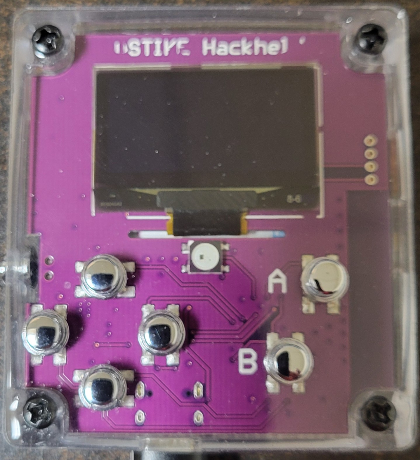
Figure 3.1 — Hackheld V1 front. Photo, 2026-05-15.
3.2 The OLED display
The display panel is a 0.96″ 128×64 monochrome SSD1306-based module. Verifiable facts from the photo:
- Active area visible as a black rectangle inside a slightly larger panel substrate.
- FPC ribbon at the bottom of the panel exiting toward the PCB.
- Markings visible on the panel substrate near the bottom — “8284AA80” or similar (panel manufacturer’s lot code; not the SSD1306 part number itself, which is on the controller IC under the panel).
The SSD1306 is an extremely common controller IC for small monochrome OLEDs. Specs:
Table 1 — The SSD1306 is an extremely common controller IC for small monochrome OLEDs. Specs
| Spec | Value |
|---|---|
| Resolution | 128 × 64 (some 0.96″ panels are 128 × 32 — verify by what Spacehuhn renders on the unit; the deauther firmware assumes 128 × 64 by default) |
| Colours | Monochrome (one colour per panel — DSTIKE’s variant appears white in the unit photo) |
| Interface | I²C or SPI per the panel variant. The Hackheld’s panel uses I²C (confirmed by the lack of separate MOSI/SCK + CS lines on the FPC; 4-wire I²C is standard for SSD1306 in this form factor). |
| I²C address | 0x3C (default) or 0x3D (variant). Adafruit_SSD1306 library default is 0x3C — match if you write custom code. |
| Backlight | None — OLED pixels emit their own light; no separate backlight to drive. |
| Power | 3.3 V logic; current draw scales with the number of pixels lit. All-black is 5 mA; all-white is ~30 mA. Watch this when running on battery. |
The SSD1306 has a known burn-in tendency at full contrast over long periods. The Deauther firmware mitigates by reducing contrast and inverting periodically; if you write custom firmware that leaves a static image on screen for hours, dim or blank the display when idle.
3.3 The seven-button cluster
Counting from the front-view photo:
Table 2 — Counting from the front-view photo
| Position | Likely role | Likely GPIO (verify) |
|---|---|---|
| Top-centre (above OLED) | RESET — pulses the EN line | Hardware, not a GPIO |
| Centre-top of cluster | UP | GPIO 12 |
| Centre-bottom of cluster | DOWN | GPIO 13 |
| Centre-left of cluster | LEFT | GPIO 0 (also FLASH-mode strap — long-press at boot enters bootloader) |
| Centre-right of cluster | RIGHT | GPIO 2 |
| Right-side A | A key — accept / enter on most firmwares | GPIO 14 |
| Right-side B | B key — back / cancel on most firmwares | GPIO 16 |
The exact GPIO map is not officially published in a clean datasheet for the Hackheld V1. It is encoded in the matching DSTIKE-fork of the Spacehuhn firmware’s A_config.h. The table above is the most plausible map based on (a) which ESP8266 GPIOs are physically available, (b) which are safe at boot (so the LEFT key + the FLASH strap on GPIO 0 is a known design choice in many similar boards), and (c) which library defaults the Spacehuhn firmware uses. Treat it as a hypothesis until verified by reading the source or putting a multimeter on the buttons one at a time.
FLASH + RESET: enter the ESP8266 ROM bootloader. The accepted choreography on this board (per universal ESP-12 convention):
1. Hold LEFT (FLASH-mode key, ground on GPIO 0)
2. Press and release RESET (pulse EN low)
3. Release LEFT
4. The chip is now in UART boot mode and will accept esptool.py / Arduino IDE upload
The bootloader is in mask ROM; this entry method is invariant across all ESP8266 silicon revisions and is the recovery path for any bricked flash state. Vol 9 § Recovery.
3.4 Silkscreen branding and serial markings
Visible silk on the front:
- “DSTIKE Hackheld” — banner, centered top
- “A” — label to the right of the A button
- “B” — label to the right of the B button
Visible silk on the back (Figure 3.2):
- “DSTIKE WiFi+” — top of the RF module
- “MODEL ESP8266MOD” — RF module
- “VENDOR www.dstike.com” — RF module
- “ISM 2.4 GHz” — RF module
- “PA = 25 dBm” — RF module (the headline)
- “802.11 b/g/n” — RF module
- “LRD” — to the right of the LiPo connector pad on the back PCB; meaning unconfirmed (likely a designator or batch code)
- ZON.CELL battery sticker QR + part info — on the cell itself, not the PCB
No serial number is silk-printed on the PCB itself. For inventory tracking, use the FCC ID of the RF module (likely registered to DSTIKE / Travis Lin — check the FCC mark on the module’s silver can for the ID) as the closest thing to a manufacturer-traceable identifier. The serial_number field in the inventory entry is blank for that reason — there is no canonical serial on this device.
3.5 Back of the board
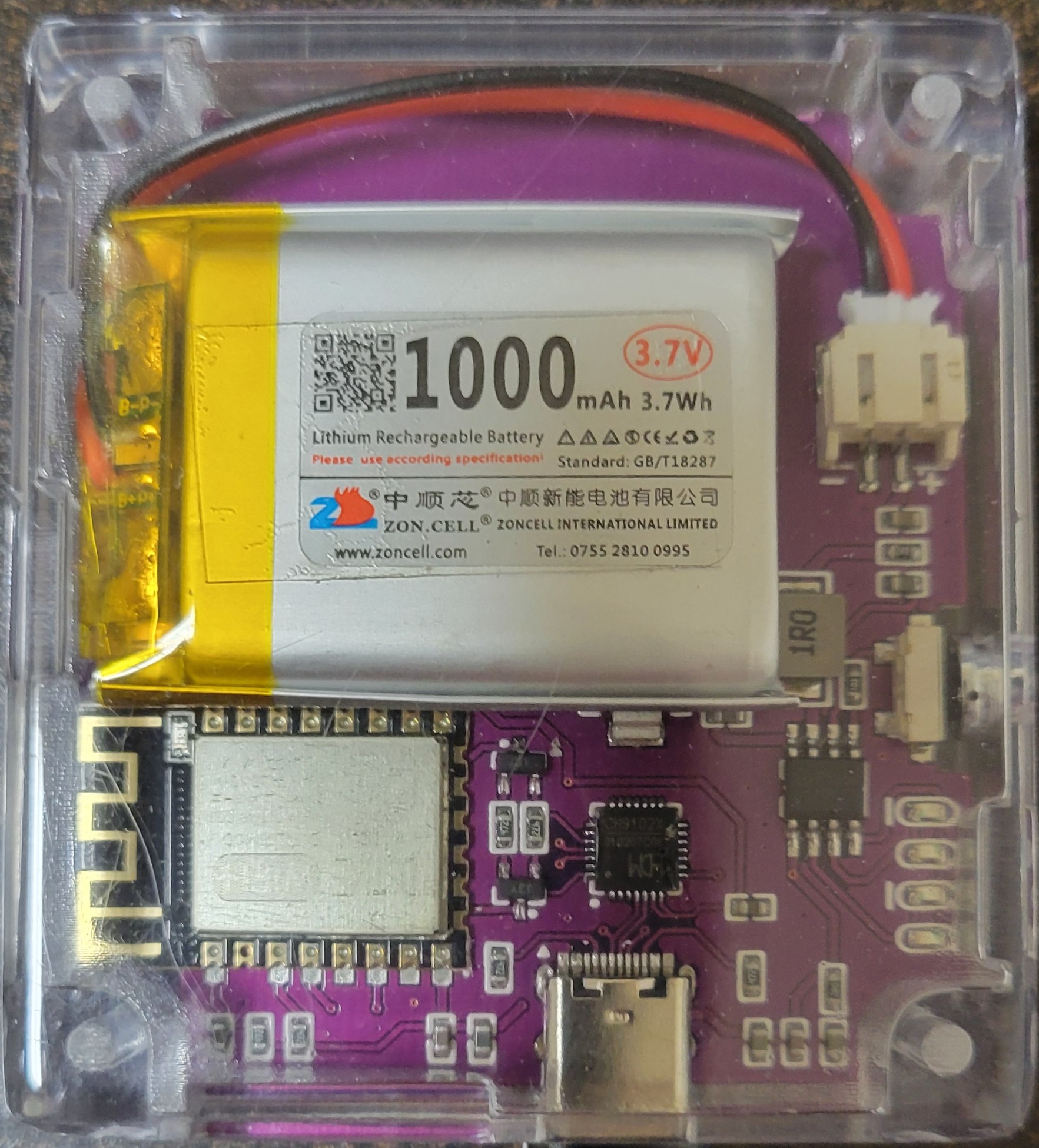
Figure 3.2 — Hackheld V1 back. Photo, 2026-05-15.
Visible features from top to bottom:
- ZON.CELL LiPo cell: 1000 mAh, 3.7 V, 3.7 Wh, GB/T18287 standard, yellow Kapton-tape-wrapped pouch construction.
- JST PH 2-pin connector: white shrouded header on the right edge for the LiPo’s red (+) / black (-) leads.
- DSTIKE WiFi+ RF module: silver shield can with the silkscreen markings of §4. The chip + flash + crystal + PA live under the can.
- CH340-class USB-to-serial: small QFN package to the lower-left of the RF module on the back PCB.
- Charge / protection IC area: SOT-23 and SOT-89 packages near the LiPo connector — TP4056-class charge IC + protection circuitry (Vol 4 § Charge).
- USB-C connector: at the bottom edge of the back PCB, mid-line of the board.
- Corner screws: four (matches front).
3.6 The DSTIKE WiFi+ RF module
Headline IC. From the silkscreen (Figure 2.1, zoomed):
Table 3 — Headline IC. From the silkscreen (Figure 2.1, zoomed)
| Item | Value |
|---|---|
| Product name | DSTIKE WiFi+ |
| Model designation | ESP8266MOD |
| Vendor | DSTIKE (www.dstike.com) |
| Operating band | ISM 2.4 GHz |
| Maximum TX power | PA = 25 dBm (~316 mW) — the differentiator |
| Standards | 802.11 b / g / n |
| Regulatory | FCC mark on the shield can |
The module form factor is ESP-12-class (same pinout). The functional upgrade vs a stock ESP-12-F is the addition of a discrete RF power amplifier in the shielded portion of the module — DSTIKE doesn’t publish the exact PA part, but it’s typical of the “ESP-12-PA” or “ESP-12-S+PA” class of upgraded modules common in this market segment.
Under the can: ESP8266EX silicon, 40 MHz crystal, 4 MB SPI flash (typical for the ESP-12-F base form factor), RF matching network, and the PA stage.
3.7 The USB-C connector
Bottom edge of the back PCB. The connector is a USB-C 24-pin receptacle, but as a CHARGE + SERIAL port (not USB-PD, not USB 3.x), only 4 pins are functionally connected:
- 5V power in (to the charge IC)
- GND
- D+ to the CH340
- D- to the CH340
USB-C connectors in this configuration are commonly described as “USB-C 2.0” or “USB-C charging” — they have the physical convenience of the reversible USB-C plug without the higher-speed or USB-PD features. The Hackheld’s design choice here is sensible: the ESP8266 is a 12 Mbps full-speed-via-CH340 device that wouldn’t benefit from USB 3.x bandwidth, and the cell is a 1000 mAh single LiPo that doesn’t need 100 W of PD negotiation.
Practical implications:
- Use any USB-C cable (USB 2.0, USB 3.x, or USB-PD) — the Hackheld will pull what it needs (under 1 A in worst case during attack TX).
- Most USB-C-to-USB-C cables work fine. A few cheap USB-C cables lack the CC pull-ups required for the receptacle to enumerate as a target device; if your laptop doesn’t see the Hackheld, try a different cable before suspecting the unit.
- The connector is not USB-OTG — you can’t plug a USB keyboard into the Hackheld and have it act as a host. ESP8266 has no USB-host capability.
3.8 The CH340 USB-to-serial IC
Small QFN visible on the back PCB. The CH340 family (CH340C, CH340N, CH340G, CH9102, etc. — DSTIKE doesn’t publish which) is a single-chip USB-to-UART bridge by WCH (Nanjing Qinheng Microelectronics). Function:
- Converts the host’s USB-CDC traffic into UART (TX/RX/optional flow control).
- Wires its UART output to the ESP8266’s UART0 (GPIO 1 = TX, GPIO 3 = RX).
- Wires its DTR + RTS lines through the auto-reset RC circuit so that Arduino IDE /
esptool.pycan pulse FLASH + RESET in software (eliminating the need to do the manual button dance on every upload).
Driver story:
Table 4 — Driver story
| OS | Driver |
|---|---|
| Linux | Mainline ch341 driver, auto-loaded. Device shows as /dev/ttyUSB0 (or higher). |
| macOS | Mainline (recent macOS versions). Older macOS needs the WCH-provided kext. Device shows as /dev/cu.usbserial-XXXX. |
| Windows 10/11 | Mainline driver auto-installs from Windows Update or via the WCH-provided installer (wch-ic.com). Device shows as COMx. |
Common driver pitfalls:
- A counterfeit CH340 will sometimes refuse to enumerate on macOS even with the latest driver. Try a different USB cable, a different port, or in extreme cases a different driver version. WCH publishes drivers per OS version; check theirs first.
- The CH340 enumerates with a vendor-default VID/PID that doesn’t tie back to DSTIKE —
1A86:7523is the most common. This means every CH340-class device on the same host fights over the same/dev/ttyUSB0namespace. For multi-device setups, useudevrules (Linux) orIORegistryExplorer(macOS) to bind to specific serial numbers.
3.9 The charge / protection circuitry
Visible as a cluster of SOT-23 / SOT-89 packages on the back PCB, near the LiPo JST connector. The Hackheld design follows the standard single-cell LiPo charger reference design:
Table 5 — Visible as a cluster of SOT-23 / SOT-89 packages on the back PCB, near the LiPo JST connector. The Hackheld design follows the standard single-cell LiPo charger reference design
| Block | Likely IC | Role |
|---|---|---|
| Linear charge controller | TP4056 (SOP-8) or equivalent | Constant-current / constant-voltage charge from USB-C 5V to 4.2V cell terminal. Typical charge current 1 A; the Hackheld board likely caps at 500 mA or so given the cell size. |
| Cell protection (over-discharge / over-current / short-circuit) | DW01 + 8205A pair, or one of the modern integrated equivalents (FS312F, etc.) | Sits between the charge IC’s output and the JST connector. Cuts the cell off if voltage drops below ~2.5V (over-discharge) or current spikes above ~3 A (short circuit). Protects the cell from the most common failure modes. |
| 3.3V LDO for ESP8266 | AMS1117-3.3 or similar | Drops the cell’s 3.0–4.2V range to a clean 3.3V rail for the ESP8266 and the OLED. ~500 mA capability (matches the worst-case peak current draw under attack TX). |
The exact IC part numbers are not silk-printed at the size visible in the unit photo. The architecture, however, is canonical — every cheap-LiPo-handheld design uses this same three-block topology. Vol 4 has the full power-tree.
3.10 The LiPo cell
The ZON.CELL sticker is highly legible in the back photo:
Table 6 — The ZON.CELL sticker is highly legible in the back photo
| Field | Value |
|---|---|
| Brand | ZON.CELL (Zoncell International Limited, Shenzhen-area; tel 0755-2810-0995; web zoncell.com) |
| Capacity | 1000 mAh |
| Nominal voltage | 3.7 V |
| Energy | 3.7 Wh |
| Standard | GB/T18287 (Chinese national standard for portable lithium-ion / lithium-polymer cells; the Chinese equivalent of UN 38.3 testing) |
| Form factor | Pouch (soft-pack) with yellow Kapton tape wrap |
| Connector | JST PH 2-pin, red (+) / black (-) leads |
| QR code | Yes, on the cell sticker — likely encodes the manufacturer’s batch info; not user-actionable |
Replacement guidance: any 1000 mAh single-cell LiPo with JST PH 2-pin (or with that connector swapped on) will fit. Look for cells around 60 × 35 × 5 mm to physically fit the cavity. Pick a cell with built-in protection — the board has cell-protection circuitry, but a cell with its own protection PCB built into the pouch is the belt-and-suspenders option for a device you might leave on a charger for weeks.
⚠️ LiPo safety: Do not puncture, crush, or short-circuit this cell. Do not leave the device in direct sun or in a car interior on a hot day (LiPo electrolyte ignites at ~150 °C). Do not charge a swollen cell — replace it. Standard lab-LiPo discipline applies; see ../_shared/legal_ethics.md for the project-wide lab safety convention.
3.11 Enclosure and mechanicals
The clear acrylic / cast-resin shell is the standard DSTIKE handheld enclosure for this revision — two halves screwed together at the corners. The window over the OLED is integrated into the front half; the cutout for the USB-C connector + the button shafts is integrated into the front half similarly. Replacement shells are not typically a stocked item; if the case cracks, the practical path is to 3D-print a replacement (the STL files exist informally on the DSTIKE Discord and on community Thingiverse mirrors).
Approximate overall dimensions (estimated from the photos; verify with calipers):
Table 7 — Approximate overall dimensions (estimated from the photos; verify with calipers)
| Dimension | Estimate |
|---|---|
| PCB | ~60 × 60 mm |
| Overall enclosed | ~75 × 75 × 25 mm |
| Weight | ~90 g with battery |
The four corner screws are M2 self-tappers in plastic standoffs molded into the case. Don’t over-torque them — the plastic strips at moderate force.
3.12 Replacement parts and BOM
If a component fails:
Table 8 — If a component fails
| Component | Replacement spec | Source |
|---|---|---|
| LiPo cell | 1000 mAh single-cell with JST PH 2-pin (or rewire connector) | Hobbyist battery store (HobbyKing, Adafruit, Tindie BatterySpace) |
| SSD1306 OLED | 0.96″ 128 × 64 I²C SSD1306, white or blue, address 0x3C | Adafruit, Amazon, AliExpress — generic part |
| Tactile button | 4-pin SMD tactile, 4×4×1.5 mm, 5 N actuation | Mouser / DigiKey / generic |
| USB-C connector | 24-pin USB-C receptacle, 12-pad SMD with 4 PTH legs | Mouser / generic |
| CH340 | CH340C QFN-10 (most common in this size) | LCSC / WCH direct |
| TP4056 charger | TP4056 SOP-8 with cell-protection daughter circuitry | LCSC / generic |
| ESP8266 module | ESP-12-F (functional substitute; loses the PA boost) or an ESP-12-PA variant (preserves the boost). Direct DSTIKE WiFi+ replacement is buy-from-DSTIKE only. | LCSC for generic; DSTIKE Tindie for the WiFi+ variant |
Reflow is doable on a hot plate at ~210°C for the small SMD parts. The RF module is module-level pluggable in some board revisions; on the Hackheld V1 it’s soldered down — replacement is hot-air rework, not socket-swap.
3.13 What’s next
→ Vol 4 — Power, battery, USB-serial unpacks the electrical: the charge cycle, the protection circuit, the 3.3V LDO, the brownout posture, and how the CH340 enumerates as a USB CDC device on each host OS. The runtime envelope under various firmware workloads.
Comments (0)