iCopy-X · Volume 2
iCopy-X / iCopy-XS — Hardware Tour
Case, LCD, keypad, antennas, the green PCB, the NanoPi NEO + AT91SAM7S Proxmark3 + Spartan-3 FPGA + STM32F103 stack, microSD, USB-C, battery
2.1 Why this volume exists
Vol 1 (Overview) established the headline fact that drives this entire volume: the iCopy-X is not a black-box appliance. The radio hardware, the FPGA bitstream, and the bare-metal MCU firmware running both the Proxmark3 ARM and the STM32 housekeeping MCU are all open-source — Nikola Lab released them in mid-2021 under GPL (Proxmark3 lineage) and MIT (STM32). The closed layer is the user-facing application that runs on the NanoPi NEO’s OpenWrt userland. Everything underneath that is documented down to the schematic. The community teardown at iCopy-X-Community/icopyx-teardown and the upstream-source catalog at iCopy-X-Community/icopyx-upstream cross-reference back to the Nikola-Lab GitHub org repositories — icopy_hw_main_pcb, icopy_hw_ant_pcb, icopy_hw_usb_fpc, icopy_fpga_3s_0921, and icopy_stm32 — and from those sources a complete hardware tour is possible without ever cracking a unit open.
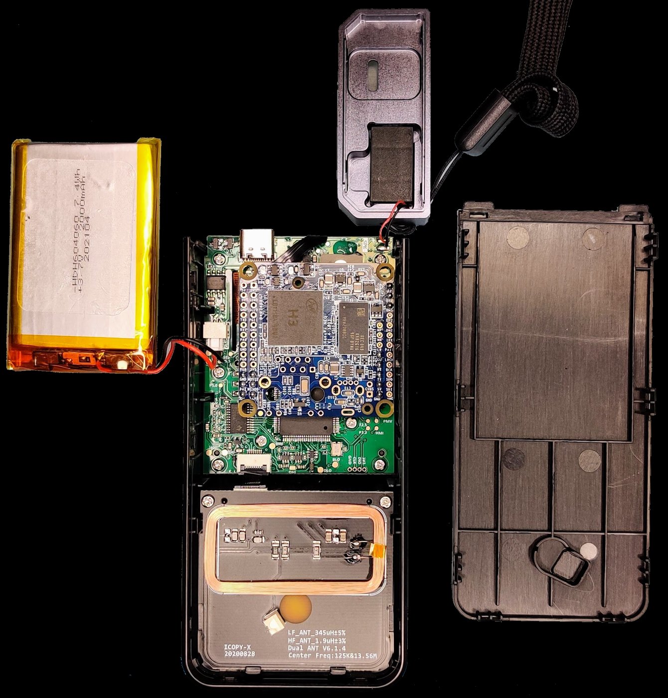
That is what this volume does. The intent is to give the reader the same mental model an engineer would have after pulling apart a unit on the bench, but built from the published schematics, Gerbers, and BOM. Where the published material is silent the volume flags the gap with a “spec confidence” note so the reader knows what is verified from sources and what is inferred. The two repos and the on-device firmware files are the load-bearing references; everything else is supporting material.
The hardware tour walks the device top to bottom — enclosure, display, keypad, the antenna PCB on the bottom face, the main “green” PCB and the parts it carries (Proxmark3 ARM, FPGA, STM32 housekeeping MCU, LCD bridge, keypad scanner, power management, USB-C), the NanoPi NEO single-board computer that hosts the Linux application layer, the FPC connector PCB that links the two, the microSD card that holds the OpenWrt image, the battery, and finally the power-on / boot sequence that pulls all of these subsystems together into a usable instrument. The point is not to document every footprint — the schematic PDFs do that — but to give the reader a coherent picture of why each subsystem is there and what its role is when the device is read-cloning a card.
The card-technology depth that uses this hardware is in Vol 3 (RFID / NFC primer) onwards; the operating-mode walk-through of how this hardware exposes itself to the user is in Vol 7 (Operating modes Part 1) and Vol 8 (Part 2); the firmware-update workflow that brings new application code onto the NanoPi NEO half of this hardware is in Vol 10 (Firmware update + open-source story). This volume is the foundation those build on.
2.2 The enclosure and form factor
The iCopy-X is a hand-held appliance the approximate size of a small TV remote: 120 × 55 × 24 mm, 113 g (specs from icopyx.com vendor page, cross-checked against multiple Lab401 product listings; spec confidence: high). The case is two-piece plastic with the seam running around the long edge; the upper half carries the LCD and keypad cutouts, the lower half is mostly transparent over the antenna PCB, with the USB-C connector cut into one short edge.
The top face has three features in a clean vertical arrangement: the 1.3-inch LCD covers roughly the upper third, a horizontal speaker grille sits immediately below the LCD on the centerline (the teardown notes call out an audio amplifier driving a speaker in the upper case section), and the four navigation buttons are arrayed underneath. The build quality is functional rather than premium — the case is the cost-down half of the bill-of-materials and is not trying to compete with industrial designs like the Proxmark3 RDV4’s Blue Shark case. The plastic is rigid enough to survive ordinary field use but the device should not be expected to take a drop from desk height onto concrete without consequences.
The bottom face is the antenna PCB itself, oriented coil-side outward. This is the surface the operator holds against a card to read or write. The two coils — one large LF loop running around the perimeter, one small HF loop in the center of the LF loop’s interior — are visible through the case material if the device is held to a strong light, which is sometimes useful for confirming antenna alignment against an unfamiliar card geometry. A small red LED is visible through the PCB during reads, providing an at-a-glance “RF is on” indication (teardown README explicitly calls this out as visible through the PCB material).
The short edges carry the USB-C port on one end (charging and host communication; see §11) and nothing on the opposite end. There is no headphone jack, no separate power switch (power is software-controlled via a long-press on one of the four buttons), and no replaceable battery compartment. The internal microSD lives behind the main PCB and is not user-accessible without case disassembly — the SD card is logically the iCopy-X’s filesystem but operationally the device is treated as having “internal storage” because the user never sees the card unless they take the device apart.
The whole package is meant to be picked up, used, and put back in a pocket. Physical robustness is adequate for indoor pentest work; outdoor or rough-handling use would warrant a small Pelican-style case or equivalent. Lab401’s product photography deliberately emphasizes the pocketability — that is the headline feature distinguishing the iCopy-X from a laptop-tethered Proxmark3 RDV4, and the form factor commits to that positioning.
2.3 The display
The display is a 1.3-inch 240 × 240 IPS-class RGB LCD, driven by the Sitronix ST7789 controller over a 4-line SPI interface. The panel part number visible on the teardown photos is BL-133H01B — a common module designation in the small-LCD supply chain for the 1.3-inch 240×240 ST7789 panel format, sold under various brand labels and substantially interchangeable across them (teardown hardware README, spec confidence: high on the ST7789 controller and the resolution; medium on the specific BL-133H01B sub-revision since multiple cosmetically-identical panels exist).
The ST7789 is the same display controller used in a wide range of small handhelds in the same era — Pimoroni and Waveshare hobby modules, several Adafruit dev boards, and many of the ESP32 dev kits. Its native interface is a 4-line SPI: clock, MOSI, chip-select, and a D/C (data/command select) line that distinguishes register writes from pixel writes. The controller carries enough on-chip RAM to hold a full 240×240 16-bit frame buffer (115.2 KB), which means the host MCU does not have to refresh the panel continuously — the host writes pixel data once and the controller handles the refresh to the panel itself. This is important for the iCopy-X’s power budget: at idle the host can put the SPI bus to sleep and the display continues to hold the last frame, with the only ongoing draw being the LCD’s own backlight and refresh circuitry.
The teardown specifically notes that the LCD interface is wired such that it can be driven by either the STM32 or the NanoPi NEO. This is a key architectural choice: it means the device can run the UI either as a NanoPi NEO Linux application (the normal mode, after the OpenWrt boot completes) or as an STM32 bare-metal application (which is useful during boot, during firmware update, and in the bare-metal Proxmark3 expert mode where the NanoPi NEO Linux side is bypassed). The arbitration between the two sides is via the on-board analog switches (the RS2105 and RS2299 SPDT/SP4T parts visible in the BOM) that route the SPI lines either way. In normal operation the NanoPi NEO renders the UI; in firmware-update or bare-metal modes the STM32 takes over.
The display’s colour rendering is adequate for the UI workload — the iCopy-X UI is mostly text and simple icons, with occasional waveform or signal-strength bargraphs during sniffing operations. There is no photographic content to render, no high-frame-rate animation. The 240×240 resolution gives about 24 characters of monospace text per line at a comfortable reading size, enough for the UID hex string of a typical RFID card plus a short status line above and below.
Backlight brightness is fixed at the firmware level — there is no user-accessible brightness control in the current 2.0 firmware family. The brightness is set high enough to read in bright fluorescent office lighting; in direct sunlight the IPS panel washes out noticeably, which is a reminder that the device is intended for indoor work.
For the curious, an ST7789 reference is straightforward: the Sitronix ST7789V datasheet (linked here for completeness; the published datasheet is the canonical authority on register-level behaviour) covers initialisation sequences, pixel-write formats, and the power-management commands the firmware uses to dim or sleep the panel. The Linux kernel running on the NanoPi NEO uses the mainline fbtft framework’s ST7789V driver, which is activated by the OpenWrt device tree overlay that the firmware update installs (the teardown notes this overlay is the iCopy-X-specific diff against a stock NanoPi NEO image).
2.4 The keypad
The keypad is four buttons in a horizontal row below the LCD, with no software-defined diagonal positions and no joystick — the absolute simplest navigation surface a multi-mode appliance can have. The buttons are commonly labelled by their function rather than by symbols: Up, Down, OK (or Select / Confirm), and Back (or Cancel / Menu). The labelling on the case differs slightly between Lab401 and Nikola Lab production batches, and some early iCopy-X units have arrows where the late iCopy-XS units have explicit labels — the function is identical across labelling variants.
Each button is mapped to a clear role across every menu in the firmware:
Table 1 — Each button is mapped to a clear role across every menu in the firmware
| Button | Default function in menu navigation | Function during card operations |
|---|---|---|
| Up | Move selection up in current list | Cycle through sub-options (e.g. card-stock type during write) |
| Down | Move selection down | Cycle the other direction |
| OK | Enter selected item / confirm action | Start the read / write / sniff operation |
| Back | Return to previous menu / cancel | Abort in-progress operation, return to home |
Long-presses extend the functionality: a long-press of OK during boot enters the bootloader / firmware-update UI; a long-press of Back at the home screen powers the device off (there is no physical power switch — the power-down is a software action gated on the long-press). The exact long-press durations are firmware-tunable; current 2.0 firmware uses approximately 1.5 seconds for power-off and approximately 3 seconds for the bootloader-recovery entry (spec confidence: medium — confirmed by community-reported behaviour but not explicitly documented in the Lab401 user manual; verify against iCopy-X-User-Manual.pdf in 05-resources/).
Mechanically, the buttons are tactile dome switches actuated through the case material — the dome lives on the green PCB underneath, with a plastic plunger transferring the press. Tactile feel is firm with a clearly defined click; the buttons are not silicone membranes (which would feel mushy) but proper tactile switches (similar to those used in industrial keypads). This makes the device usable without looking at it once the menu structure is familiar — the operator can navigate by feel during a discreet read, which matters for the field-pentest use case.
Electrically, the keypad-scan is straightforward: each button pulls one of four GPIO lines low when pressed, with weak pull-ups handling the idle state. The teardown does not pin down which MCU is the keypad master — but the architectural logic is that the STM32F103C8T6 is the always-on housekeeping controller (it survives suspend states the NanoPi NEO Linux side does not) and is therefore the most likely owner of the keypad scan. The NanoPi NEO Linux side queries the STM32 over UART for keypad events when needed. This division means the STM32 can wake the NanoPi NEO from a sleep state via a button press even when the Linux side has suspended itself.
The narrow 4-button vocabulary is a deliberate UX choice — every menu has to fit into a four-button navigation model, which forces the firmware to keep menu hierarchies shallow and consistent. The cost is that anything text-entry-like (entering hex keys, naming saved cards) requires a clumsy character-picker UI; the benefit is that the operator never has to remember what an unfamiliar button does. The Flipper Zero has the same constraint with its 5-button arrangement (D-pad + OK + Back) and resolves it the same way — short menu trees, character-picker for text. The Proxmark3 RDV4, by contrast, has no on-device UI at all — all interaction is via the laptop client — and so does not face this constraint.
2.5 The antenna PCB
The bottom face of the device is, as noted in §2, the antenna PCB itself. The PCB is silkscreen-marked with the following identifying strings, all of which are useful to know if a unit needs to be matched against schematic revisions:
ICOPY-X 20200828— board revision date (28 August 2020).LF_ANT_345uH±5%— LF coil nominal inductance 345 µH, ±5% tolerance.HF_ANT_1.9uH±3%— HF coil nominal inductance 1.9 µH, ±3% tolerance.Dual ANT V6.1.4— internal Nikola Lab antenna-PCB revision identifier.Center Freq:125K&13.56M— the two operating centre frequencies, 125 kHz LF and 13.56 MHz HF.
These markings are explicitly documented in the teardown hardware README and are the canonical reference for what the PCB is. Spec confidence: high.
2.5.1 The LF coil (125 kHz)
The LF coil is the large rectangular loop running around the perimeter of the antenna PCB. The 345 µH inductance is in the same ballpark as the Proxmark3 RDV4’s LF antenna (the RDV4’s HF/LF antennas are sold as a separate “Blue Shark” assembly, with the LF coil in a similar inductance class). The teardown notes that the iCopy-X’s antenna PCB has an “aspect quite similar to RDV4 antennas,” which is unsurprising given the Proxmark3 lineage at the silicon level.
For 125 kHz LF operation the resonance equation is:
$$f_0 = \frac{1}{2\pi\sqrt{LC}}$$
With L = 345 µH and target f₀ = 125 kHz, the resonating capacitance works out to approximately 4.7 nF. The actual matching network on the iCopy-X’s antenna PCB uses standard SMD ceramics in a parallel resonant arrangement, but the exact capacitance value is not called out in the teardown — to nail it down precisely the reader would need to fetch the antenna-PCB Gerbers from Nikola-Lab/icopy_hw_ant_pcb and read the component values from the schematic PDF (spec confidence: medium on the exact capacitance; high on the resonance principle and the approximate value).
The drive electronics for the LF coil sit on the green PCB, not on the antenna PCB itself — the antenna PCB is a passive resonant structure, with the active driver and the receive front-end on the green side. This is the standard Proxmark3 architecture: the FPGA generates the 125 kHz carrier as a switched square wave at 4.8 MHz / 38 = 125.97 kHz (the standard PM3 divisor selection), the antenna’s tank circuit shapes that into a clean sinusoid at resonance, the LF coil radiates the field, and the same coil picks up the load-modulation response from the card when it is reading.
Receive sensitivity for LF is the standard Proxmark3 chain: a CMOS Rail-to-Rail op-amp (the GS8722 dual op-amp visible in the BOM is a strong candidate for the LF receive amplifier — 11 MHz GBW, MSOP8 package, two amplifiers per part) feeds an envelope-detected signal into the FPGA, which decodes the FSK / ASK / PSK modulation patterns the various LF tag families use (Vol 4 covers those modulation patterns in detail). The detection is essentially identical to what the Proxmark3 RDV4 does — same FPGA bitstream lineage, similar analog front-end topology.
Antennas Vol 14 (transmitting loops) covers the underlying physics of small resonant loop antennas; readers interested in why the LF coil has to be physically large (to enclose enough flux for the magnetic-coupling read distance) and the HF coil can be small (because 13.56 MHz field strength falls off with the cube of distance, and the read range is consequently very short anyway) should read that volume.
2.5.2 The HF coil (13.56 MHz)
The HF coil is the smaller rectangular loop in the centre of the LF coil’s interior. At 1.9 µH and 13.56 MHz the resonating capacitance works out to approximately 72 pF, again with the exact value on the antenna-PCB schematic. The HF coil is purpose-designed for ISO 14443A/B (the MIFARE family) and ISO 15693 (iCODE, picopass, iCLASS) operation — both standards specify 13.56 MHz carrier and similar near-field coupling distances of a few centimetres.
The HF chain is more complex than the LF chain at the analog level — it has to handle higher-bandwidth modulation, including the 847.5 kHz subcarrier that ISO 14443B uses, and the various subcarrier schemes ISO 15693 uses. The TLC5510 8-bit 20 MSPS ADC visible in the BOM is the HF receive digitizer — it samples the IQ-demodulated baseband from the HF coil and feeds the FPGA, which then handles the protocol-level decoding (subcarrier recovery, bit-clock recovery, frame-format decoding). The 20 MSPS sampling rate is enough headroom to oversample the 847.5 kHz subcarrier comfortably and to handle the higher data rates (424 kbps, 848 kbps) that the more recent ISO 14443 cards use.
For transmit, the HF coil is driven the same way as the LF coil — the FPGA generates the carrier as a switched square wave, the antenna’s tank circuit shapes it, and the coil radiates. The transmit path uses the RS2105 and RS2299 SPDT/SP4T analog switches to route between the LF and HF driver chains, since the same FPGA pins drive both at different frequencies under different mode-selection state.
2.5.3 The interconnect
The antenna PCB connects to the green PCB via an 8-pin FPC (flexible printed circuit) cable. The 8 pins carry: LF coil drive (differential), HF coil drive (differential), LF receive, HF receive, an LED control line for the on-PCB red LED, and ground/shield returns. The exact pinout is in the icopy_hw_ant_pcb schematic PDF; the teardown notes the 8-pin FPC count but does not enumerate each wire individually.
The FPC connector is a common surface-mount FPC socket with a flip-lock retention mechanism. Replacing the antenna PCB (e.g. after a damaged coil from a heavy drop) is in principle a 5-minute job once the case is open — flip the lock, slide the FPC out, slide the new one in. In practice no one does this because the antenna PCB is not sold as a spare part by Lab401 — a damaged antenna PCB means a returned unit.
2.6 The main “green” PCB — overview
The green PCB is the system integration board — the densest, most interesting piece of the iCopy-X from an electronics-engineering standpoint. Its silkscreen identifies it as ICOPY MAIN V1.5 D-2110 — V1.5 board revision, manufacturing date code 2110 (October 2021). It carries every active component on the iCopy-X with the exception of the NanoPi NEO (which is a separate SBC, see §10) and the LCD module (which is a separate panel-on-flex assembly connected via a small ribbon to a header on the green PCB).
The active components on the green PCB include the Proxmark3 RF front-end stack (Atmel AT91SAM7S512 ARM + Xilinx Spartan-3 FPGA + W25Q80 SPI flash for the FPGA bitstream + various op-amps and analog switches), the STM32F103C8T6 housekeeping MCU, the LCD driver interface (a small bridge of analog switches and SPI buffer logic that lets either the STM32 or the NanoPi NEO drive the LCD), the keypad-scan inputs, the power supply chain (IP5305 power-bank SoC + TPS61170 boost + XC9236 buck + TLV70012 / TLV70025 LDOs + battery-charge management), the USB-C connector and bridge logic, and the audio amplifier for the speaker.
A clean conceptual decomposition of the green PCB is:
┌─────────────────────────────────────────────────────────────────────────────┐
│                          GREEN PCB (V1.5)                                   │
│                                                                             │
│  ┌─────────────────┐    ┌──────────────────┐   ┌──────────────────────┐     │
│  │  Proxmark3 RF   │    │  STM32F103C8T6   │   │  Power management    │     │
│  │  ────────────   │    │  ──────────────  │   │  ─────────────────   │     │
│  │  AT91SAM7S512   │◄──►│  Housekeeping:   │   │  IP5305 power-bank   │     │
│  │  + Spartan-3    │    │  LCD/keypad/     │   │  + boost + buck      │     │
│  │  XC3S100E FPGA  │    │  audio/charge    │   │  + LDOs              │     │
│  │  + W25Q80 flash │    │  status          │   │  + USB-C charging    │     │
│  │                 │    │                  │   │                      │     │
│  └────────┬────────┘    └────────┬─────────┘   └──────────────────────┘     │
│           │ USB                  │ SPI/UART                                  │
│           │                      ▼                                          │
│   ┌───────▼────────────────────────────────┐    ┌──────────────────────┐    │
│   │  20-pin + 24-pin header to NanoPi NEO  │    │  Antenna PCB FPC     │    │
│   │  (14 of 44 pins actually wired)        │    │  (8 lines)           │    │
│   └────────────────────────────────────────┘    └──────────────────────┘    │
│           │                                                                 │
│   ┌───────▼─────────┐  ┌──────────────────┐    ┌──────────────────────┐     │
│   │  4-pin FPC      │  │  LCD bridge      │    │  Speaker + amplifier │     │
│   │  to USB-C       │  │  (analog mux)    │    │  (K318 audio amp)    │     │
│   └─────────────────┘  └──────────────────┘    └──────────────────────┘     │
│                                                                             │
└─────────────────────────────────────────────────────────────────────────────┘
The next subsections walk each block.
2.7 The Proxmark3 stack — AT91SAM7S512 + Spartan-3 + W25Q80
The single most architecturally significant fact about the iCopy-X is this: the RFID work is done by a Proxmark3. Not “a Proxmark3-like circuit” — an actual Proxmark3, with the same MCU silicon, the same FPGA part family, the same op-amp / ADC analog front-end topology, the same firmware lineage, and the same FPGA bitstream lineage. The assignment-level scaffold in the previous session described the iCopy-X’s RFID brain as “an STM32 MCU above an FPGA”; the teardown corrects that — the RFID brain is an Atmel AT91SAM7S512 (ARM7TDMI) running the Proxmark3 firmware codebase, and the STM32F103C8T6 is a separate housekeeping MCU that does not participate in the RFID datapath.
This matters because the same Iceman-fork Proxmark3 community that maintains the Proxmark3 RDV4 firmware also maintains the firmware lineage that runs inside the iCopy-X — which is why Nikola Lab was obligated to release their modifications under the Proxmark3 GPL, and why the iCopy-X’s RF capabilities track the Proxmark3 capability frontier so closely. New attacks added to Proxmark3 mainline (a new MIFARE Plus key-recovery technique, a new HID Prox variant) propagate to the iCopy-X firmware on the next firmware update — sometimes with a lag of months, sometimes promptly, depending on Lab401’s release cadence (Vol 10 §4).
2.7.1 AT91SAM7S512 — the Proxmark3 ARM
The AT91SAM7S512 is Atmel’s (now Microchip’s) ARM7TDMI microcontroller in the SAM7S product family — 55 MHz max clock, 512 KB internal flash, 64 KB internal SRAM, USB device peripheral, multiple UARTs, SPI, two PWM units, and the ADC needed for the Proxmark3 RF receive chain. It is the canonical Proxmark3 MCU; every Proxmark3 generation from the original Proxmark3 Easy through the Proxmark3 RDV4 has used some variant of this part. The “512” in the part number is the flash size in KB — earlier Proxmark3 generations used the SAM7S256 (256 KB flash), and the RDV4 moved up to the 512 to fit the expanded firmware codebase. The iCopy-X uses the 512 variant, consistent with the contemporary Proxmark3 capability set (teardown hardware README, spec confidence: high — explicitly identified in the teardown).
The AT91SAM7S512 in the iCopy-X has JTAG not routed and JTAG disabled — the silicon’s JTAG security fuse is blown at the factory, and the JTAG pins are not even exposed on the PCB. This is conventional Proxmark3 production practice and is not specific to the iCopy-X; Lab401’s RDV4 production units have the same configuration. The implication is that you cannot reflash the AT91SAM7S512 over JTAG even if you crack the case open — you have to use the standard Proxmark3 firmware-flash workflow, which goes over USB and uses the on-chip bootloader. The firmware-update mechanism in Vol 10 handles this transparently from the user’s perspective.
The AT91SAM7S512 communicates with the NanoPi NEO over USB — the SAM7S’s USB device peripheral enumerates as a Proxmark3 CDC-ACM serial device, exactly as it would on a laptop-tethered RDV4. The NanoPi NEO’s Linux side opens this as /dev/ttyACM0 (or similar) and talks the Proxmark3 wire protocol to it. The application software on the NanoPi NEO is a wrapped Proxmark3 client — it sends Proxmark3 commands over the USB-CDC pipe and receives responses, then turns those responses into LCD updates and audio cues for the user. In Expert Mode / Proxmark Mode (Vol 8 §5) the application gets out of the way and the user types raw Proxmark3 client commands; the wire protocol is identical to what an RDV4 user types into the laptop client.
2.7.2 Xilinx Spartan-3 XC3S100E FPGA
The FPGA in the iCopy-X is a Xilinx Spartan-3 XC3S100E — the smallest member of the Spartan-3E family, with 100K equivalent logic gates, 4 block-RAMs, and an order-of-magnitude smaller die than the Spartan-6 / Artix-7 parts that came later. The teardown explicitly identifies the part as “another unlabeled FPGA, possibly a Spartan 3”; the Verilog upstream repo at Nikola-Lab/icopy_fpga_3s_0921 confirms it is the XC3S100E specifically — the directory name is icopy_fpga_3s_0921 (the “3s” is Spartan-3 family designation) and the synthesized bitstream targets the XC3S100E part (spec confidence: high — cross-checked between teardown observation and the upstream Verilog repo’s synthesis configuration).
The XC3S100E choice is the standard Proxmark3 FPGA, not an iCopy-X-specific selection. The Proxmark3-RRG mainline maintains the FPGA bitstream as the fpga-xc3s100e/ directory — the iCopy-X’s Verilog was merged into that subdirectory in August 2021, and the iCopy-X’s firmware loads the same bitstream image at boot. The bitstream does the time-critical RF work: it generates the LF and HF carrier waveforms (as switched square waves at the right divisor of the 24 MHz reference clock), it handles the digital-filter front-end on the receive side, it does the bit-clock recovery and the modulation demodulation, and it presents a clean byte-level interface up to the AT91SAM7S512.
The bitstream is stored in an external W25Q80 8 Mbit SPI flash (the 8C7I5 USON2x3 part in the teardown BOM is the W25Q80BLUXIG variant). At power-on, the FPGA reads its bitstream from this flash over SPI, configures itself, and signals the AT91SAM7S512 that it is ready. The bitstream is updated as part of the firmware-update process — a new firmware image can include a new FPGA bitstream, which the AT91SAM7S512 will rewrite into the W25Q80 during the update. This is standard Proxmark3 practice.
The XC3S100E is small by modern standards — a single Spartan-6 or Artix-7 part in the same logic-gate range as the original Proxmark3 ARM-plus-FPGA combination would be a single-chip solution today. But the Proxmark3 lineage carries the Spartan-3 forward because (a) the part is still in production and is cheap, (b) the Verilog ecosystem around it is mature, and (c) changing FPGAs would force a re-validation of years of accumulated Proxmark3 RF-modem code. Lab401 inherits all three reasons and uses the same XC3S100E in the iCopy-X.
2.7.3 W25Q80 SPI flash
The W25Q80BLUXIG (Winbond 8 Mbit / 1 MB SPI NOR flash, USON-2×3 package, the 8C7I5 BOM line) is the FPGA bitstream storage. 1 MB is plenty of room for a Spartan-3 XC3S100E bitstream (which is ~80 KB after synthesis and compression) with multiple bitstream variants stored side-by-side. The Proxmark3 firmware historically uses two bitstreams — one tuned for LF operation, one for HF — and selects between them at runtime depending on the operation being performed; the iCopy-X inherits this dual-bitstream model.
The same W25Q80 also serves as overflow storage for Proxmark3 firmware data that does not fit in the AT91SAM7S512’s 512 KB internal flash — selected card-emulation data tables, decoder lookup tables, and similar. The exact partition layout is in the Proxmark3 firmware source (armsrc/ in mainline).
2.7.4 The analog front-end
The receive chain components visible in the teardown BOM include:
- OPA355NA (TI 200 MHz GBW CMOS single op-amp, SOT-23-6
C55) — the high-bandwidth front-end amplifier for the HF receive path. - GS8722 (11 MHz GBW dual CMOS op-amp, MSOP8
TE29BA) — likely the LF receive amplifier (the bandwidth is overkill for 125 kHz but the part is widely available and cheap; the LF path needs the gain). - TLC5510IPW (TI 8-bit 20 MSPS pipeline ADC, TSSOP24
Y5510 78T A1JH) — the HF baseband digitizer, sampling the IQ-demodulated baseband at 20 MSPS for the FPGA to process. - SN74LVC2G17DCKR (dual Schmitt-trigger buffer, SOT-23-6
C7F DCK-6) — clock-signal cleanup, probably on the LF coil drive path. - BAV99 (dual fast-switching diode, SOT-23
A7) — likely diode clamping on the receive input to protect the op-amp from high transient voltages when the transmit pulse switches off. - RS2105 (SPDT analog switch, MSOP10) and RS2299 (quad SPDT, QFN-3×3-16L) — the bus-routing switches that select between LF and HF datapaths and between STM32-control and NanoPi-control of various signals.
This combination is, again, conventional Proxmark3 practice. The component choices are cost-optimized versions of equivalent Proxmark3-RRG / Proxmark3 RDV4 parts. A reader who has the Proxmark3 RDV4 schematic side-by-side with the iCopy-X main PCB schematic will see broadly the same architecture with cost-down substitutions in the analog ICs.
2.8 The STM32F103C8T6 — the housekeeping MCU
The STM32F103C8T6 is the housekeeping microcontroller on the green PCB. The teardown’s initial pass described its role as “still to figure out” — community work after the teardown has clarified that it handles the LCD bridge (when the NanoPi NEO is not driving the LCD directly), the keypad scan, the audio interface, the battery-charge status / power-management signalling, and the inter-processor communication with the NanoPi NEO over UART.
It is not part of the RFID datapath. The RFID work is entirely the AT91SAM7S512 + FPGA combination described in §7. The STM32 sits outside that path and handles all the “everything else” that a portable appliance needs.
2.8.1 The part
The STM32F103C8T6 is the ubiquitous “Blue Pill” MCU — ARM Cortex-M3 at 72 MHz, 64 KB flash, 20 KB SRAM, multiple SPI / I²C / UART, three 12-bit ADCs, USB device peripheral, an RTC. The “C8T6” variant is the 48-pin LQFP package. The part has been a workhorse in the maker community for over a decade and is one of the cheapest fully-capable Cortex-M MCUs available. The choice here is entirely about cost — the STM32F103 does everything housekeeping the iCopy-X needs, at a per-unit cost of well under a dollar.
The teardown notes that the STM32 has RDP1 (Read-Out Protection level 1) enabled, which prevents straightforward firmware extraction over JTAG / SWD. The teardown author managed a partial firmware dump (~89% of the firmware contents) using the Exception(al) Failure attack against the STM32F1 RDP1 — a published academic technique that exploits an interrupt-handling weakness in the F1’s RDP implementation. This work is summarized in the teardown STM32 README along with the modifications to the public stm32f1-firmware-extractor tool that were needed to run the attack on a live iCopy-X (the iCopy-X needs to be powered during the attack, not just JTAG-connected, so the tool was modified to use soft resets instead of hard resets).
That partial dump aside, the STM32’s full firmware source has now been released — Nikola Lab published it as Nikola-Lab/icopy_stm32 under the MIT license in August 2021. So the firmware is available without resorting to the RDP attack; the attack was useful in the period before the source release and is now a forensics curiosity.
2.8.2 What the STM32 firmware does
Reading the public icopy_stm32 source, the STM32 firmware’s responsibilities are:
- LCD bridge management — at boot, the STM32 owns the LCD. It renders the boot splash, the bootloader / firmware-update UI (if invoked), and any low-level error screens that need to be shown before the NanoPi NEO Linux side has come up. Once the NanoPi NEO is ready, the STM32 hands the LCD over via the analog-switch routing described in §3.
- Keypad scan — the STM32 polls the four keypad GPIOs, debounces the inputs, decodes long-presses and short-presses, and forwards key-events to the NanoPi NEO over UART (UART0 in the teardown’s pinout table, on STM32 pins 30 (RX) and 31 (TX)).
- Audio output — the STM32 generates the beep tones and short audio cues the device emits during card reads and writes. The audio amplifier (the K318 BGA part — a Redmi 4A ringing IC by repurpose) is driven from an STM32 PWM output. The NanoPi NEO can also drive audio (it has lineout-left wired to the same amplifier, see the teardown pinout table) for longer / richer audio output during full-Linux operation.
- Battery-charge management coordination — the STM32 monitors the IP5305 power-bank SoC’s status outputs and the battery voltage, and reports charge state to the NanoPi NEO over UART.
- Inter-processor communication — the STM32 ↔ NanoPi NEO UART (115200 8N1, by convention) is the main control channel. The NanoPi NEO can ask the STM32 “what was the most recent key event?” and the STM32 can asynchronously notify “battery is low, please shutdown cleanly.”
- Power-on / power-off sequencing — the STM32 is the always-on controller. When the device is “off,” the STM32 is in low-power sleep with the wake source set to the keypad’s OK long-press; the NanoPi NEO and everything else is fully powered down. When the OK long-press wakes the STM32, the STM32 enables the main power rails, releases the NanoPi NEO’s reset line, and the boot sequence (§13) takes over from there.
The MIT-licensed source release makes all of this directly verifiable — anyone can clone icopy_stm32 and read the firmware. The “untested” tag on the upstream repo’s STM32 firmware entry refers to the build / flash workflow not having been validated end-to-end by the community (it requires the closed-source toolchain that Nikola Lab uses internally, plus the right STM32 flash tool); the source-code authenticity is not in doubt.
2.8.3 The companion icopy_time_synchronizer tool
The Nikola-Lab/icopy_time_synchronizer project is a small MIT-licensed utility for setting the STM32’s RTC (real-time clock) from a host computer over USB. It uses the CSerialPort library (an LGPL fork of a serial library). The RTC keeps the iCopy-X’s date/time across power cycles, which matters for the firmware-update workflow (the per-device .ipk update package is timestamped) and for the log-keeping the Linux side does. This is a minor utility but useful context — there is a documented host-side communication path with the STM32, distinct from the AT91SAM7S512’s USB-CDC path, that the community could in principle build other tools against.
2.9 Power management
The iCopy-X’s power tree is built around the IP5305 as the master power-bank SoC, with a chain of downstream regulators feeding the various subsystems.
2.9.1 The IP5305
The IP5305 is a fully-integrated power-bank system-on-chip — it combines a Li-ion charger (1.2 A charge current), a synchronous boost converter (1.0 A boost), battery-protection, fuel-gauge approximation, and the input/output switching for USB charge-in and 5 V power-out. Power-bank SoCs of this class are produced by a handful of Chinese semiconductor houses (Injoinic, FitiPower, and similar) for the consumer power-bank market; their cost-per-unit at volume is low and their feature integration is high, which makes them attractive for portable consumer electronics.
In the iCopy-X, the IP5305 is the bridge between the USB-C charging input, the 2000 mAh LiPo battery, and the 5 V rail that feeds the rest of the device. When the USB-C is plugged in and supplying power, the IP5305 charges the battery (at up to 1.2 A) and supplies the 5 V rail from the USB input. When unplugged, the IP5305 boosts the battery’s 3.0–4.2 V output to a regulated 5 V to feed the rest of the device.
2.9.2 Downstream regulators
The 5 V output from the IP5305 feeds:
- TPS61170DRVR — a 1.2 A high-voltage boost converter (output up to 38 V, the part’s headline use is white-LED driver / OLED bias generation). On the iCopy-X this is probably driving the LCD backlight LED string (LCD backlights typically need 15–25 V) (spec confidence: medium — inferred from the part type and the absence of any other obvious LCD-backlight driver in the BOM; verify against the main PCB schematic).
- XC9236B38DMR — a 3.8 V step-down PWM/PFM buck converter, 600 mA, 3 MHz switching frequency. This is one of the main 3.8 V rails — likely feeding the NanoPi NEO (which is normally a 5 V part but accepts 3.8–5.5 V on its VIN with adequate regulation), or alternatively a 3.8 V intermediate rail that the LDOs hang off (spec confidence: medium).
- TLV70012DCKT and TLV70025DCKT — 200 mA low-IQ low-dropout regulators producing 1.2 V and 2.5 V output respectively (the part-number suffix encodes the voltage). These are the precision rails feeding the FPGA core voltage (the XC3S100E needs 1.2 V Vccint) and the FPGA / AT91SAM7S512 / STM32 I/O voltages (3.3 V is typical for those parts, although the 2.5 V LDO may be feeding a different sub-circuit; the exact mapping is on the main PCB schematic).
The cascaded regulator chain is conventional — a master buck/boost produces an intermediate rail, low-noise LDOs produce the precision sub-rails. The LDOs are chosen for low quiescent current (the “Low IQ” designation in their part names) to keep the standby battery drain low when the device is “off” but the STM32 is still in keep-alive sleep waiting for the OK long-press.
2.9.3 The battery
The battery is a LiPo 604060 3.7 V 7.4 Wh 2000 mAh cell (teardown hardware README — spec confidence: high). The “604060” designator is the cell-format code: 6 mm thick, 40 mm wide, 60 mm long. This is a common laptop-replacement / handheld-electronics cell format. The 2000 mAh capacity at 3.7 V nominal gives the 7.4 Wh energy, which is enough for several hours of active RFID operation (RFID receive is low-current; transmit is higher but is duty-cycled in 100% of normal use cases).
The cell is wired with standard JST-connector or solder-tab termination to the IP5305’s BAT input. No user-accessible battery replacement — pulling the case apart and de-soldering is the only path, which is generally only done when the cell has aged past usefulness (3+ years of heavy field use).
2.9.4 USB-C charging
The USB-C connector on the green PCB is wired through a 4-pin FPC to the NanoPi NEO’s micro-USB footprint (see §10.2 for the FPC bridge detail). The USB-C provides three functions:
- Charging input — VBUS through a regulator that feeds the IP5305’s charging input.
- USB data — the D+/D- lines route through the FPC to the NanoPi NEO’s USB peripheral, exposing the NanoPi NEO Linux side over USB to a connected host. This is how the firmware-update workflow puts a new .ipk file onto the device.
- Host-side USB to the Proxmark3 ARM — separately, the AT91SAM7S512’s USB peripheral can be accessed via a different mechanism (the exact routing depends on which USB endpoint mode the device is in; in Expert Mode the AT91SAM7S512 enumerates directly as a Proxmark3 device, but the wire-level details are not pinned down in the teardown).
The USB-C is not Power Delivery (PD) — it is a 5 V-only USB-C connection using the basic CC pull-down convention. There is no negotiation for higher voltages; the input is straight 5 V at up to whatever current the host supplies (typically 1.5 A from a modern phone charger, more than enough for the IP5305’s 1.2 A charge current).
2.10 The NanoPi NEO
The NanoPi NEO is the Linux application processor — the SBC that runs OpenWrt, the Lab401 application bundle, and the user-facing UI on top of the AT91SAM7S512 Proxmark3 layer.
2.10.1 The board
The standard NanoPi NEO V1.4 from FriendlyARM is a 40 × 40 mm SBC built around the Allwinner H3 quad-core Cortex-A7 SoC at 1.2 GHz, with 256 MB or 512 MB DDR3 RAM (two SKU variants), a micro-SD slot for boot, USB-A and USB micro-USB, 10/100 Ethernet, and 24-pin + 12-pin GPIO headers. The iCopy-X uses an OEM variant of the NanoPi NEO: same SoC and memory, but without the Ethernet jack, USB-A port, or the 12-pin extra header — only the 24-pin and 20-pin headers are present, and only 14 of those 44 pins are actually connected (teardown NanoPi NEO README, spec confidence: high). The variant ships as a stripped-down OEM SKU available to volume customers like Lab401.
The Allwinner H3 is a well-trodden SoC — it appears in dozens of cheap Allwinner-based SBCs and Android TV sticks, has mature mainline Linux support, and its peripheral set (multiple UARTs, SPI, I²C, USB host/device, audio codec, Mali-400 GPU) is more than the iCopy-X needs. The H3 runs the Lab401 application as ordinary Linux userspace code — Python and Node.js stack, by community report, with the application UI handling the LCD render via the kernel’s fbtft ST7789V driver and keypad events arriving over the UART link to the STM32 (§8).
2.10.2 The interconnect to the green PCB
The NanoPi NEO connects to the green PCB through two paths:
- A 20+24-pin header pair — physically a pair of 0.1″ pin headers on the NanoPi NEO’s edge, mating with sockets on the green PCB. Despite the header count of 44 pins total, only 14 pins are actually wired (teardown table). The wired pins carry: USB D+/D- to the AT91SAM7S512’s USB device port, SPI0 to the LCD driver (so the NanoPi NEO can drive the LCD directly when it owns the bus), UART0 for the inter-processor link to the STM32, audio lineout-left for the speaker amplifier, 5 V power in (from the IP5305), and ground.
- A 4-pin FPC to the USB-C connector — wired from the green PCB’s USB-C through an FPC bridge to the NanoPi NEO’s micro-USB footprint, giving the NanoPi NEO Linux side a host-facing USB connection (the firmware-update path).
The architectural picture is: the NanoPi NEO is the brain of the user-facing application, the AT91SAM7S512 is the brain of the RFID work, the STM32 is the housekeeping coordinator, and the three communicate over (a) USB-CDC NanoPi-to-AT91SAM7S, (b) UART NanoPi-to-STM32, and (c) shared SPI buses for the LCD (with analog-switch arbitration).
2.10.3 The microSD card
The NanoPi NEO boots from a 16 GB microSD card that lives in the internal slot. The card partition layout is documented in the teardown as:
Table 2 — The NanoPi NEO boots from a 16 GB microSD card that lives in the internal slot. The card partition layout is documented in the teardown as
| Partition | Size | Filesystem | Contents |
|---|---|---|---|
mmcblk0p1 | 40 MB | FAT32 | U-Boot bootloader |
mmcblk0p2 | 1.7 GB | ext4 | OpenWrt rootfs |
mmcblk0p3 | 1.5 GB | ext4 | overlay userdata (writable overlay on rootfs) |
mmcblk0p4 | 11 GB | FAT (no number — large data partition) | ICOPY-X data partition — saved card dumps, application state, logs |
The U-Boot variant is U-Boot SPL 2017.11, customized by Nikola Lab from the stock FriendlyARM NanoPi NEO U-Boot. The rootfs is the FriendlyCore Xenial-based image (Ubuntu 16.04 LTS for ARMHF) with Nikola Lab’s customizations layered on. The customizations identified by the teardown are: debug-port moved from ttyS0 to ttyS1, the ST7789V LCD driver activated in the device tree overlay, and a minor init-script change to the rootfs initramfs. The application bundle proper is delivered as .ipk packages on top of the OpenWrt rootfs — this is what the firmware-update workflow installs and updates.
The 16 GB card is large enough to hold the OS plus tens of thousands of saved card dumps (a typical full HF card dump is a few KB; a typical LF tag dump is even smaller). Capacity is not a constraint on field use.
2.11 The USB-C bridge
The USB-C connector is the only external port on the device. It is wired through a small FPC connector PCB (Nikola-Lab/icopy_hw_usb_fpc on Nikola Lab’s upstream) that bridges between the USB-C connector’s physical receptacle on the green PCB and the NanoPi NEO’s micro-USB footprint internally. The bridge PCB is a tiny board carrying just the USB-C receptacle, the CC pull-down resistors that signal a USB-C-to-USB-A or USB-C-to-USB-C cable, and the FPC connector that runs to the green PCB.
Functionally the USB-C delivers:
- 5 V charging input through VBUS to the IP5305.
- USB data to the NanoPi NEO’s micro-USB peripheral, for the firmware-update workflow (the host computer talks to the NanoPi NEO Linux as a USB-tethered network device).
- Through a separate routing path within the green PCB, USB-CDC access to the AT91SAM7S512 when the device is in Expert / Proxmark mode.
The USB-C connector is mechanically robust — it is a standard USB-C receptacle SMT part rated for thousands of insertion cycles. The FPC bridge means the receptacle is replaceable in principle (de-solder the bridge PCB, install a new one) without disturbing the rest of the device, although this is not a documented field repair.
The lack of USB Power Delivery (PD) negotiation is worth flagging: the device will charge from any 5 V USB-C source (phone chargers, laptop USB-C ports, power banks) but will not negotiate for fast-charge profiles. This is a deliberate cost choice — adding a PD controller would have added chip-count and complexity for a benefit (faster charging) that the use case did not require.
2.12 The speaker and audio amplifier
The speaker is a small moving-coil speaker mounted in the upper section of the case (teardown hardware README — “Casing with a speaker in the top part”). It is driven by the K318 audio amplifier, which is identified in the teardown BOM as a Redmi 4A ringing IC — a low-cost mobile-phone audio amplifier repurposed for the iCopy-X’s audio output.
The audio chain has two possible input sources: the STM32’s PWM output (used for the beep tones during reads / writes, the boot chime, and short error cues) and the NanoPi NEO’s audio lineout-left (used for any audio output the Linux side wants to produce — though in practice the Lab401 application produces very little audio beyond what the STM32 already provides). The two inputs are routed to the K318 through the analog-switch network (RS2105 / RS2299) the same way the LCD bridge is.
The speaker is not loud enough to be useful in noisy environments and is not intended to be — its purpose is short, near-field confirmation tones, not music playback or general audio. Most operators turn the audio off in firmware settings; the LCD’s visual feedback is sufficient.
2.13 The power-on / boot sequence
Bringing all the subsystems together, the iCopy-X’s boot sequence runs as follows:
- Long-press OK on the keypad. This is the device’s only “power-on” input.
- STM32 wakes from its low-power sleep, detects the OK long-press meets the duration threshold, and enables the main power rails (the XC9236 buck, the LDOs, the NanoPi NEO’s VIN).
- STM32 takes the LCD — drives the boot splash to the ST7789 via SPI. The user sees the iCopy-X / Lab401 boot logo.
- STM32 releases the NanoPi NEO’s reset line. The NanoPi NEO’s Allwinner H3 begins its boot ROM execution.
- U-Boot SPL runs from the SD card’s first partition. It does basic hardware initialization (DDR3 RAM training, peripheral setup) and chains to the main U-Boot.
- Main U-Boot loads the Linux kernel from the boot partition and starts the kernel with the iCopy-X device tree overlay (which activates the ST7789V LCD driver in the kernel).
- Linux kernel boots. Standard OpenWrt / FriendlyCore initialization. The kernel takes the LCD over from the STM32 (analog-switch routing flips), and the boot splash transitions to the Linux-side application splash.
- The Lab401 application starts as a userspace process (init.d or systemd, depending on which OpenWrt variant). The application opens a UART connection to the STM32 for keypad events and audio control, opens a USB-CDC connection to the AT91SAM7S512 for Proxmark3 commands, and waits for the FPGA to finish loading its bitstream from the W25Q80.
- AT91SAM7S512 powers up, reads the FPGA bitstream from the W25Q80 over SPI, configures the Spartan-3 XC3S100E, and reports “Proxmark3 ready” to the NanoPi NEO over USB-CDC.
- Application enters its main loop — the user sees the home menu, can navigate with the keypad, and can begin RFID operations. The entire sequence from OK long-press to home menu is approximately 15–25 seconds on a fully-discharged-then-charged unit; faster on a unit that has been used recently (cache effects in the Linux file system).
Power-off is the inverse: a long-press of Back at the home menu triggers a clean shutdown — the application unwinds, Linux halts, the STM32 cuts the power rails to the NanoPi NEO, and the STM32 returns to its low-power sleep with the next OK long-press as the wake source. A forced power-off (long-press of Back held for an extreme duration, or simultaneous Back+OK) bypasses the clean shutdown — usable if the application has hung, but should be avoided since it can corrupt the SD card’s filesystem (the overlay userdata partition is ext4 and is moderately tolerant of unclean shutdowns, but corruption is possible).
The boot sequence is documented in operational depth in Vol 10 §3 (firmware update workflow) — the firmware-update process inserts itself between steps 6 and 7 (with a special U-Boot variable set) and is the only standard way the operator interacts with the boot sequence.
2.14 What the teardown does not document
The published teardown and the published Nikola Lab upstream repositories cover the hardware and the bare-metal MCU firmware exhaustively. They do not cover:
- The Lab401 / Nikola Lab application bundle on the NanoPi NEO. This is the closed-source layer — the Python and Node.js code that implements the user-facing UI, the menu structure, the operating modes, and the iCS Decoder Tool integration. The application is delivered as
.ipkpackages bound to per-device serial numbers (so the package that updates a specific iCopy-X cannot be transferred to a different unit) and is what the firmware-update workflow updates. - The iCS Decoder Tool’s firmware-licensed unlock logic. The iCS Decoder is a paid add-on (Vol 6 §5) that enables iCLASS SE / SEOS decoding. The mechanism is presumed to be a per-device licence stored in the application bundle (the iCS Decoder package is a separate .ipk install that the firmware-update workflow handles), but the exact licence-validation mechanism is not documented.
- Any “tamper detection” or “anti-cloning” measures Nikola Lab may have built into the AT91SAM7S512 firmware. The AT91SAM7S has its security fuses blown, JTAG is disabled, and the firmware update path is the only documented way to put new code on the device. Whether there are runtime checks the firmware does on its environment is not publicly known.
- The specific RTC battery / coin cell behaviour for keeping the STM32 RTC alive across full battery discharge. The community has not documented whether there is a separate RTC backup cell or whether the RTC is simply lost on full discharge.
- The specific assembly tolerances for the LF and HF coil resonance at the manufacturing line. The published
±5%and±3%tolerances on the coil inductances are bins, not necessarily centred values; a unit could be at one edge of its bin and tune slightly differently from a sister unit. This is academic for field-pentest work but matters for anyone considering re-tuning the matching networks (which would be a research-grade exercise more appropriate for a Proxmark3 RDV4 anyway).
These gaps are listed for honesty — the teardown is excellent but it is not exhaustive, and a reader who wants to understand every detail will eventually need to crack open their own unit and verify against the schematic. For the level of detail needed to use the iCopy-X effectively, the gaps do not matter.
2.15 Summary — the seven things to remember
- The RFID brain is a Proxmark3 — Atmel AT91SAM7S512 ARM + Xilinx Spartan-3 XC3S100E FPGA + W25Q80 SPI flash for the bitstream. This is the same architecture as the Proxmark3 RDV4, with cost-down analog-front-end substitutions.
- The Linux application brain is a NanoPi NEO — Allwinner H3 quad-core Cortex-A7 at 1.2 GHz, 256 MB RAM, OEM variant without Ethernet/USB-A. It runs OpenWrt with Lab401’s closed-source application bundle on top.
- The housekeeping MCU is a separate STM32F103C8T6 — handles LCD bridge, keypad scan, audio output, battery-charge coordination. Not part of the RFID datapath. Firmware open-source under MIT at
Nikola-Lab/icopy_stm32. - The antenna PCB is the bottom face — LF coil 345 µH at 125 kHz, HF coil 1.9 µH at 13.56 MHz, both on a single board, both connected to the green PCB via an 8-pin FPC.
- The LCD is an ST7789 240×240 in a 4-line SPI configuration — dual-master capable (either STM32 or NanoPi NEO can drive it), with the routing arbitrated by the on-board analog switches.
- Power is an IP5305-based power-bank chain plus a 2000 mAh LiPo 604060 battery, USB-C 5 V charging (no PD), and a cascade of LDOs for the precision sub-rails.
- The published open-source story makes the radio hardware verifiable — schematics, FPGA Verilog, and STM32 firmware are all open. The Linux application layer is closed, and the firmware-update workflow is per-device-serial-bound, which is the structural lock-in with Lab401 (Vol 10 §4).
The next volume (Vol 3 — RFID / NFC primer) takes this hardware foundation and explains the physics and protocols the iCopy-X uses it for: LF magnetic coupling and the EM4XX / HID Prox / T5577 modulation patterns, HF inductive coupling at 13.56 MHz and the ISO 14443A/B / 15693 protocol stacks, and the boundary cases — why some tag families crack open with darkside attacks in seconds and others require nested-hardnested key recovery taking hours, why iCLASS SE and SEOS need a separate decoder, why ISO 14443B is technically supported but practically rare in access-control work.
References
- iCopy-X-Community teardown — hardware README — the canonical hardware-internals reference, with the silkscreen markings, the visual BOM, the interconnect tables.
- iCopy-X-Community teardown — NanoPi NEO README — the SBC and microSD-card layout reference.
- iCopy-X-Community teardown — STM32 README — the housekeeping-MCU reference, including the RDP1 partial-firmware-extraction work.
- iCopy-X-Community upstream catalogue — the index of what Nikola Lab has released open-source.
- Nikola-Lab/icopy_hw_main_pcb — the main PCB schematics and Gerbers.
- Nikola-Lab/icopy_hw_ant_pcb — the antenna PCB schematics and Gerbers.
- Nikola-Lab/icopy_hw_usb_fpc — the USB-C bridge FPC PCB.
- Nikola-Lab/icopy_fpga_3s_0921 — the FPGA Verilog source.
- Nikola-Lab/icopy_stm32 — the STM32F103 firmware source (MIT-licensed).
- Proxmark3-RRG fpga-xc3s100e/ — the upstream Proxmark3 mainline FPGA directory where the iCopy-X Verilog has been merged.
- Sitronix ST7789V datasheet — the LCD controller datasheet (one of several mirrors).
- This subproject’s local resources:
05-resources/iCopy-X-User-Manual.pdf,05-resources/Update your iCopy-X _ ICopyX.pdf,05-resources/iCS Decoder for iCLASS® SE _ SEOS Decoder — Lab401.pdf. - Sibling tool deep dive — laboratory counterpart: Proxmark3 RDV4.
- Sibling tool deep dive — antenna fundamentals: Antennas Vol 14 (transmitting loops).
Comments (0)