Bus Pirate 6 · Volume 9
Bus Pirate 6 Volume 9 — Workflows: SPI Flash Dump, EEPROM, JTAG Pin-Find, DDR5 SPD, Smart Card
End-to-end recipes — clip-on vs desolder, dump and verify, the offline-DIMM SPD workflow, SLE4442 read/write with PSC
9.1 About this volume
These are the end-to-end practical recipes — combining the protocol modes from Vols 6-7 with the adapters from Vol 8 — that you actually run on the bench. Each section walks a complete workflow from “I have a target board / chip / card in front of me” to “I have the data on disk.”
The recipes assume you’ve read Vols 1-8. They cross-reference back liberally rather than repeating background.
9.2 SPI flash dump workflow — end to end
The single most common BP6 workflow. You have a SPI flash chip (BIOS / UEFI / IoT-router firmware / dev-board flash); you want to dump it, possibly modify it, and write it back.
9.2.1 Identify chip package (SOIC / DIP / WSON)
Look at the chip with a 10× loupe and identify the package:
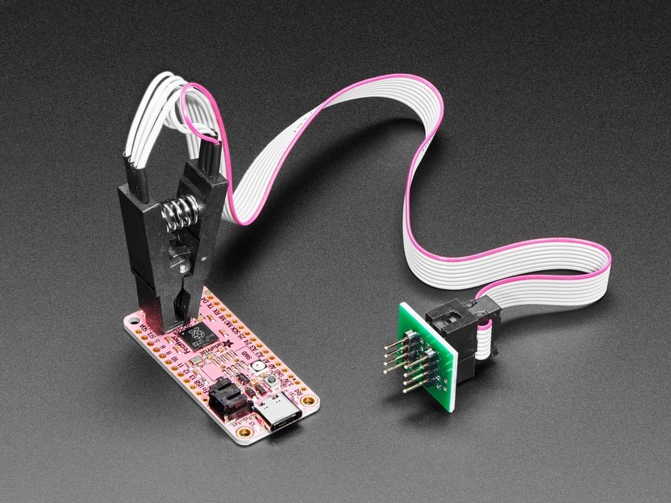
- SOIC-8 (small outline, 150 mil or 208 mil wide, 8 leaded pins) — most common modern flash. Visible leads on both sides. → SOP8 adapter (Vol 8 § 5) for desoldered chips, or Pomona 5250/5252 clip for in-circuit.
- DIP-8 (dual in-line, through-hole, 0.3″ pitch) — vintage / dev-board flash. Pins go through holes. → DIP8 adapter (Vol 8 § 4).
- WSON-8 / DFN-8 (small outline, no leads, flat pads on underside, 5×6 mm or 6×8 mm) — modern BIOS / UEFI / router flash. No visible leads. → WSON8 adapter (Vol 8 § 3), out-of-circuit only.
If the chip is unmarked or you can’t tell the package, photograph it with a quarter for scale and check flashrom’s chip database or the BP6 firmware’s database — you may be able to match by approximate dimensions.
9.2.2 Choose adapter vs clip (decision tree)
Is the chip currently soldered to a board?
├── No (you have a bare chip)
│   └── Pick adapter by package: SOP8 / DIP8 / WSON8
└── Yes (chip is on a target board)
    └── Is in-circuit reading acceptable for this target?
        ├── Yes (target has the SPI chip's CS, MOSI, MISO, CLK exposed
        │        and you can isolate them — typically by holding the
        │        target's main CPU in reset to prevent bus contention)
        │   └── SOIC-8 → Pomona 5250 (150 mil) or 5252 (208 mil) clip
        │       DIP-8 → less common in-circuit; usually need to desolder
        │       WSON-8 → NOT possible (no leads to clip onto) — must desolder
        └── No (target's bus is too crowded, or you want forensic copy)
            └── Desolder + use adapter by package
The “hold the target’s main CPU in reset” trick is the key to in-circuit reading. Without it, the target’s CPU drives the SPI bus during boot and contends with the BP6’s drive. With it, the CPU is off-bus and the BP6 has the bus to itself.
9.2.3 In-circuit vs out-of-circuit decision
In-circuit (clip-on) advantages:
- No desoldering — chip stays on board, no risk of damage.
- Faster — clip on, dump, clip off.
- Reversible — original device still works.
In-circuit disadvantages:
- Some target boards have parallel buffers / muxes on the SPI bus that interfere.
- Some target CPUs can’t be held in reset reliably (no exposed RESET pin, or RESET also resets the flash).
- Power-during-read can be tricky (some boards’ flash chips share a regulator with the CPU; powering the chip means powering the CPU).
Out-of-circuit (desolder) advantages:
- Always works regardless of target board electrical complications.
- Faster sustained reads (no parallel buffer overhead).
- Cleaner forensic copy — exact bit-for-bit dump.
Out-of-circuit disadvantages:
- Requires hot-air rework station (or a steady hand with two soldering irons for SOIC-8).
- Risk of damaging the chip or PCB pads during desolder/resolder.
When in doubt: try in-circuit first with a Pomona clip. If it doesn’t work cleanly (CRC errors, partial reads), switch to desolder.
9.2.4 Connect, power, identify (JEDEC ID readback)
Once the chip is in the adapter (or the clip is on the chip):
- BP6 to SPI mode:
m→ 6 → wizard. Accept defaults (Mode 0, 1 MHz to start). - Set the PSU voltage to match the chip’s VCC:
W 3.3(or 1.8 / 5 depending on the chip’s datasheet). - Confirm voltage:
v— verify VOUT reads as expected. - Identify the chip: at the SPI prompt, type
flash. The BP6 issues a JEDEC ID command (0x9For0x90) and decodes:
SPI> flash
Reading manufacturer/device ID...
Manufacturer: 0xEF (Winbond)
Device: 0x4018 (W25Q128 - 16 MB)
Capacity: 16 MiB
Sector size: 4 KB
Page size: 256 B
If JEDEC ID is 0x00/0xFF or all-zeros — connection problem. Verify:
- Power good?
- Adapter / clip seated firmly?
- WP pin tied high? (some chips lock without it)
- HOLD pin tied high? (same)
If ID returns but isn’t in the firmware database — fall through to flashrom (§ 2.7) which has a broader database.
9.2.5 Dump → save → verify
The canonical dump:
SPI> flash dump w25q128_backup.bin
Reading 16,777,216 bytes...
Progress: 100% [################]
Read complete: 16 MB to /captures/w25q128_backup.bin
SHA256: a3d9c8b1f6e21c14...
The file lands on the BP6’s NAND filesystem at /captures/. Pull it off via USB MSC (drag-and-drop from the mounted drive on the host).
Always verify:
SPI> flash verify w25q128_backup.bin
Reading and comparing...
Progress: 100% [################]
Match confirmed.
If verify reports mismatches, do not write back any modifications — the dump is unreliable. Re-check connections and re-dump.
9.2.6 Edit and write back
Modify the dumped binary on the host (hex editor, custom patcher, firmware mod tool). Then drop the modified file back onto the BP6 NAND:
SPI> flash write modified_image.bin
Reading current chip contents...
Comparing with new image...
Erasing 47 affected sectors (4 KB each)...
Writing 47 sectors × 16 pages × 256 B = 192 KB total...
Verifying...
Write complete and verified.
The BP6’s smart flash write only erases sectors that differ from the new image, then programs only the differing pages. Much faster than chip-erase-then-write, and reduces wear on the chip.
If you want a forced full-chip-erase-then-write:
SPI> flash erase
Are you sure? Chip-erase is irreversible. Type "yes":
yes
Erasing entire chip...
SPI> flash write modified_image.bin
[writes from scratch — every sector / every page]
9.2.7 flashrom integration via BBIO
For chips the BP6 firmware’s built-in database doesn’t recognize, or for workflows that need flashrom’s full feature set (coreboot integration, advanced write-protect register manipulation, the broader chip database):
# On the host, after entering BBIO mode on the BP6:
flashrom --programmer buspirate_spi:dev=/dev/ttyUSB0,spispeed=4M \
    -r dump.bin
flashrom finds the BP6 via the buspirate_spi programmer driver, identifies the chip via its own database, and writes the dump to the host filesystem.
For write-back via flashrom:
flashrom --programmer buspirate_spi:dev=/dev/ttyUSB0,spispeed=4M \
    -w modified.bin
flashrom handles erase + write + verify in one command.
Note: spispeed=4M is a reasonable starting clock; for chips that support it, 8M or 16M works and dumps faster.
9.3 Logic-analyzer capture of the dump (BP6-only)
The BP6’s defining capability (Vol 2 § 5). Capture every clock edge and data byte during a flash dump for verification, forensic documentation, or understanding non-standard chip behavior.
9.3.1 Setting up the 8T245 look-behind capture
The 74LVC8T245 buffer (Vol 2 § 5.1) and the dedicated PIO state machine (Vol 3 § 6.4) are always running in BP6 firmware — they aren’t a separate mode. To capture the data they’re sampling:
- Connect to the BP6 via a second USB-CDC port (USB enumerates multiple endpoints). The first is the CLI; the second is for binary protocols.
- Enter binary mode menu:
binmodeat the CLI prompt. - Select option 2 (BPIO2) or option 3 (SUMP — for sigrok / PulseView compatibility).
For PulseView, SUMP is the easier path because PulseView speaks SUMP natively.
9.3.2 PulseView client + BPIO2 integration
The PulseView workflow:
- BP6:
binmode→ SUMP (option 3). The BP6’s second USB-CDC port now speaks SUMP. - Host: launch PulseView. Add a new device, select “Openbench Logic Sniffer (SUMP)” as the driver, point at the BP6’s second COM/tty port.
- PulseView connects, identifies the 8 channels (IO0-IO7).
- Set capture rate (4-50 MHz typical for SPI flash dump work).
- Add a SPI protocol decoder on the relevant channels (CLK, MOSI, MISO, CS).
- Click “Run” to start capture.
- On the BP6 (back at the CLI on the first USB-CDC port): run
flash dump. The dump proceeds; PulseView captures in parallel. - After the dump completes, in PulseView: stop capture. The screen shows every byte that crossed the bus, decoded by the SPI protocol analyzer.
The result is a byte-for-byte verifiable record of the dump — useful for forensic work where you need to prove the contents weren’t tampered with, or for understanding a non-standard chip’s behavior (timing quirks, unexpected wait states).
This is impossible on BP5 / BP5XL — they can drive or sample, but not both on the same pin.
9.4 I²C EEPROM (24-series) workflow
After SPI flash, I²C 24-series EEPROM is the second-most-common dump workflow. 24-series EEPROMs (24LC256, 24C32, 24FC512, etc.) store config / calibration / serial-number data on countless embedded devices.
9.4.1 24LC256 / 24C32 worked example
For a 24LC256 (32 KB / 256 Kbit, I²C address 0x50, 16-bit sub-address):
HiZ> m
Mode> 5 (I²C)
[wizard: 100 kHz, pull-ups on, 7-bit address]

I2C> scan
Found device at 0x50

I2C> eeprom read 0x50 0x0000 32768
Reading 32,768 bytes from EEPROM at 0x50...
Progress: 100%
Saved to /captures/eeprom_0x50.bin
SHA256: ...
The eeprom command in I²C mode (Vol 6 § 4.5) handles the sub-address width and page-boundary logic automatically.
For 24C32 (4 KB / 32 Kbit, I²C address 0x57, 8-bit sub-address):
I2C> eeprom read 0x57 0x00 4096
[same flow, 4 KB dumped]
9.4.2 Page-write timing
24-series EEPROMs require 5 ms between writes for internal programming (the cell-write time, not the bus-write time). The eeprom write command builds this delay in:
I2C> eeprom write 0x50 0x0000 4 0x11 0x22 0x33 0x44
Writing 4 bytes...
Waiting for write cycle (5 ms)...
Write complete.
If you build raw bracket sequences instead, add D:6 (6 ms — slightly conservative) between every write transaction.
For page writes (writing more than 1 byte per transaction — 24-series chips allow up to 64 bytes per page in their page-program mode), eeprom write automatically pages-up the writes to respect the chip’s page-size boundary.
9.4.3 Address pin (A0/A1/A2) discovery
24-series EEPROMs have 3 hardware-address pins (A0, A1, A2), tied to GND or VCC at PCB level, that select between 8 possible I²C addresses (0x50 + 0…7 = 0x50-0x57). Multiple EEPROMs on one bus all use 0x5X but with different A0/A1/A2 wiring.
If you don’t know which addresses are populated:
I2C> scan
Found device at 0x50
Found device at 0x51
Found device at 0x52
That’s three EEPROMs on the bus (A0/A1/A2 settings 000, 001, 010). Dump each separately:
I2C> eeprom read 0x50 ...
I2C> eeprom read 0x51 ...
I2C> eeprom read 0x52 ...
9.5 Microwire EEPROM (93-series) workflow
Older / niche. 93C46, 93C56, 93C66, 93C76, 93C86 — 1 Kbit to 16 Kbit Microwire serial EEPROMs. Found on older PC motherboards, automotive ECUs, some legacy embedded designs.
Microwire is a 3-wire protocol (CS, CLK, DI/DO — sometimes 4 wires with separate DI and DO). The BP6 supports it via 3-Wire mode.
HiZ> m
Mode> 8 (3-Wire / Microwire)
[wizard: pick chip family, set CS polarity]

3WIRE> mwire read 93C46
Reading 128 bytes (16-bit organization)...
Saved to /captures/eeprom_93c46.bin
The mwire command knows the major 93-series chip families and their per-chip command sets. For unsupported chips, fall back to raw 3-Wire transactions in the syntax language.
9.6 JTAG pin-find workflow (blueTag)
This is the workflow Vol 5 § 7 introduced. The end-to-end version:
9.6.1 Identifying header pads on unknown boards
You sit down at an unfamiliar board. There’s a 4-pin / 6-pin / 8-pin header (with or without silkscreen labels). You suspect debug; you don’t know which pins.
Step 1: Identify candidate pads. Pads that are obviously NOT debug:
- Power rails (typically wide traces, often labeled VCC / V3.3 / V5 / GND)
- GPIO with LEDs (labeled LED1 etc.)
- External clock crystal pads (paired pins with small SMD parts between)
- Test points marked TP## with no debug context
Pads that are likely debug:
- In a row of 4-8 with no obvious external connections
- Close to the main MCU (debug headers are usually 1-2 cm from the SoC)
- No silkscreen labels, but obviously placed for cable attachment
Step 2: Power the target. Either:
- Apply external power via the target’s own power input.
- Or use the BP6’s PSU at the target’s rail voltage (
W 3.3for most modern MCUs).
9.6.2 Scan procedure with the BP6’s 8 probes
- Connect probes IO0-IO7 to the candidate pads (you can leave unused IOs floating if there are fewer than 8 candidates).
- Connect GND to a known ground.
- Enter JTAG mode (
m→ 12). Accept defaults for the setup wizard. - At the JTAG prompt:
bluetag
JTAG> bluetag
Powering target sense...
Scanning 8 candidates × possible TCK/TMS/TDI/TDO arrangements...
Progress: 12% (TCK candidate IO0)...
Progress: 25% (TCK candidate IO1)...
...

[after 5-30 seconds]

bluetag scan complete
JTAG interface found:
  TCK = IO3
  TMS = IO5
  TDI = IO2
  TDO = IO4
IR length: 4
IDCODE: 0x3BA02477
  Vendor: ARM Ltd.
  Part:   Cortex-M3
9.6.3 IDCODE → chip identification
The 32-bit IDCODE decodes into vendor / part / revision via the firmware’s built-in database (see Vol 7 § 2.2). Common decodings:
0x3BA02477— ARM Cortex-M3 (the example above)0x4BA00477— ARM Cortex-M40x0BA01477— ARM Cortex-M00x4BA02477— ARM Cortex-M7
For more obscure parts, look up the raw 32-bit IDCODE in any of the public JTAG IDCODE databases — JEP106 vendor codes are the standardized prefix.
9.6.4 OpenOCD handoff with the discovered pinout
After bluetag identifies the pinout, reconfigure JTAG mode to use those exact pins:
JTAG> m
Mode> 12 (JTAG)
[setup wizard: pin assignments]
TCK pin: IO3
TMS pin: IO5
TDI pin: IO2
TDO pin: IO4
TRST pin: (none / disable)
[other defaults]

JTAG> openocd
Entering OpenOCD bridge mode. BBIO protocol active on USB-CDC.
Connect OpenOCD on host.
On the host:
openocd -f interface/buspirate.cfg \
    -c "buspirate_port /dev/ttyUSB0; buspirate_speed normal; buspirate_vreg 1" \
    -f target/stm32f1x.cfg
OpenOCD connects, identifies the target chip (or uses the user-supplied target config), and you have a full debug session — register read/write, flash programming, GDB attachment via target remote :3333.
9.7 SWD pin-find workflow
Same as JTAG pin-find (§ 6) but for 2-wire SWD. bluetag auto-detects whether the target speaks JTAG or SWD and reports accordingly.
If the target is ARM Cortex-M (the dominant class for SWD), the BP6 firmware tries SWD first because of its prevalence. If SWD doesn’t respond on any pin pair, falls through to JTAG scanning.
Once identified:
JTAG> bluetag
Scanning for SWD interfaces...
Progress: 60% (SWCLK = IO3)...

bluetag scan complete
SWD interface found:
  SWCLK = IO3
  SWDIO = IO5
DPIDR: 0x2BA01477
  Vendor: ARM Ltd.
  Part: Cortex-M4 + FPU
Reconfigure JTAG mode for SWD pins, then openocd bridge as in § 6.4. The host-side OpenOCD config changes only by adding transport select swd:
openocd -f interface/buspirate.cfg \
    -c "buspirate_port /dev/ttyUSB0; transport select swd" \
    -f target/stm32f1x.cfg
9.8 DDR5 SPD workflow
Offline DIMM Serial Presence Detect read. Useful for forensic DIMM identification, custom-timing experimentation, or recovery from a bricked vendor SPI tool.
9.8.1 DDR5 adapter plank setup
You need the DDR5 SPD I²C adapter plank (Vol 8 § 10.2). The plank has a UDIMM or SODIMM slot, level shifters, and power regulation so the DIMM works without a host motherboard.
Setup:
- Plug DDR5 DIMM into the plank.
- Plug the plank into the BP6’s main probe header.
- BP6 → I²C mode, defaults (100 kHz or 400 kHz).
The plank handles power internally — the DIMM sees its required 5 V Vdd through the plank’s regulator.
9.8.2 SPD-Hub I²C address (0x50-0x57)
DDR5 DIMMs have an I²C SPD-Hub at one of the standard EEPROM addresses (0x50-0x57). For a single DIMM, almost always 0x50. To scan:
I2C> scan
Scanning I²C bus...
Found device at 0x50
9.8.3 JEDEC EE1004 / 5118 SPD payload parse
The DDR5 SPD payload is 1 KB per JEDEC EE1004 (DDR4 was 512 bytes; DDR5 doubled it). The ddr5 command reads the full payload and parses:
I2C> ddr5
Reading 1 KB SPD payload from 0x50...
[progress bar]

DIMM info:
  Manufacturer: Micron Technology (JEP-106 0x2C)
  Part Number: MTC10F1084S1RC48BD1
  Serial: 0x12345678
  Date Code: Week 18, 2024
  Capacity: 32 GB
  Module type: UDIMM
  ECC: No

  Speed: DDR5-4800 (JEDEC default)
  CAS latency (CL): 40
  tRCD: 40 cycles
  tRP: 40 cycles
  tRAS: 80 cycles
  tRC: 120 cycles

  XMP Profile 1: DDR5-6400 CL36-39-39-78
  XMP Profile 2: DDR5-6000 CL30-36-36-77

  EXPO Profile 1: DDR5-6000 CL30-36-36-77

  Voltage: 1.1 V VDD, 1.8 V VPP

Write SPD to /captures/ddr5_micron_32gb_serial0x12345678.bin? [y/N]
Confirm y and the full 1 KB SPD goes to NAND for later analysis.
9.8.4 XMP / EXPO profile read
XMP (eXtreme Memory Profile, Intel) and EXPO (Extended Profiles for Overclocking, AMD) are pre-tested overclock profiles stored in the SPD by the DIMM manufacturer. The ddr5 parse decodes these explicitly (see § 8.3 output).
These profiles tell you what speed + timings the DIMM is rated for above its JEDEC default. Useful for:
- Identifying genuine vs counterfeit DIMMs (counterfeit DIMMs often have edited SPD profiles that don’t match the silicon).
- Sourcing replacement DIMMs (find a DIMM with matching profiles).
- Forensic confirmation of what a system was running.
9.8.5 SPD unlock + write-back (unlocked DIMMs only)
Most production DIMMs ship with the SPD write-locked at the factory — the SPD-Hub’s write-protect register prevents alterations. For custom-timing experiments, you’d need a DIMM with the SPD unlocked.
For unlocked DIMMs (rare; some “tweaker” SKUs ship unlocked), the BP6 can write back modified SPD:
I2C> ddr5 write modified_spd.bin
Writing 1 KB SPD to 0x50...
Verifying...
Done.
Don’t write back to locked DIMMs. The SPD-Hub will reject the writes (ACK the address but discard the data). Your DIMM stays correct; you’ve just wasted a few seconds. But: don’t risk it on a production DIMM you depend on — if for some reason the SPD-Hub does accept the write, the DIMM may not POST in any motherboard.
9.9 SLE4442 smart card
The full workflow for SLE4442 memory cards (Vol 7 § 5).
9.9.1 256-byte memory read (no auth needed)
HiZ> m
Mode> 7 (2-Wire)
[wizard: defaults]

2WIRE> sle4442 read
Reading 256-byte memory...

Memory dump:
0000: 02 00 14 4E 7F 70 65 73 12 34 5A B5 24 0C C0 00
0010: A1 B2 C3 D4 E5 F6 07 18 29 3A 4B 5C 6D 7E 8F 90
...
00F0: FF FF FF FF FF FF FF FF FF FF FF FF FF FF FF FF

Saved to /captures/sle4442_dump.bin
The main 256-byte memory is publicly readable — no PSC needed. The first 32 bytes are the protected area (write-protected without PSC); the remaining 224 bytes are application data.
9.9.2 PSC authentication (3 attempts before lock)
If you need to write anywhere in the card’s memory, you must first authenticate with the 3-byte PSC:
2WIRE> sle4442 read_psc
PSC location reads: 0x000000 (the card returns zeros — PSC is hidden from
readback for security, even before authentication).

Attempts remaining: 3 of 3.

2WIRE> sle4442 auth 0x123456
WARNING: This is PSC attempt 1 of 3 since the last successful auth.
3 wrong attempts permanently locks the card. Type "yes" to confirm:
yes

Auth successful. Attempt counter reset to 3.
Don’t guess PSCs unless you’re prepared to brick the card. The 3-attempt limit is hard-coded in the silicon — once you blow through it, the card is dead. There’s no recovery, no factory-reset, no override.
9.9.3 Protection-bits set / read
Each of the 32 protected-area bytes has 4 protection bits per byte:
2WIRE> sle4442 read_protection
Protection bits (one nibble per byte of the protected area):
00: F (no writes allowed)  01: F  02: F  03: F  ...  1F: F
To set a protection bit (after successful auth), use the appropriate sle4442 protect subcommand. Once set, a protection bit cannot be cleared — it’s a one-way write-protect.
Use case: program the protected area with manufacturer / serial / identification bytes, then lock them so they can’t be tampered with downstream.
9.10 ISO 7816 SIM card
Full smart-card workflow with the SIM and IC card adapter plank (Vol 8 § 10.3).
9.10.1 ATR parse
After resetting the card (via the adapter’s RST pin), the card responds with ATR:
HiZ> m
Mode> 4 (HDUART)
[wizard: 9600 baud, settings per ISO 7816]

HDUART> sim atr
Resetting card...
ATR (Answer-to-Reset):
  3B 9F 95 80 1F C7 80 31 A0 73 BE 21 13 67 43 20 0F 90 00

Decoded:
  TS (initial char): 0x3B (direct convention)
  T0: 0x9F → TA1/TB1/TC1/TD1 present, 15 historical bytes
  TA1: 0x95 → Fi=512, Di=32, max clock rate ~5 MHz at Di=32
  TB1: 0x80 → Vpp not used
  ...
  Historical bytes: 31 A0 73 BE 21 13 67 43 20 0F 90 00
  ATR matches: GSM SIM
The decoder uses the firmware’s built-in ATR database (matches against known patterns for SIM / EMV / Mifare-ULC / etc.).
9.10.2 SIM file-system walk (3F00 / 7F10 / etc.)
SIM cards use hierarchical file IDs:
HDUART> sim select 3F00       # navigate to MF (master file)
Selected 3F00 (MF). Free space: 8192 bytes.

HDUART> sim select 7F10       # navigate to DF Telecom
Selected 7F10 (DF Telecom).

HDUART> sim select 6F3A       # navigate to EF ADN (Abbreviated Dialing Numbers)
Selected 6F3A (Phone book).
Record length: 28 bytes
Record count: 250

HDUART> sim verify_chv1 1234   # present PIN1
PIN1 OK. Attempts remaining: 3.

HDUART> sim read_record 1
Record 1:
  Name: HOME
  Number: +1-555-1234
  TON: International
The hierarchy MF → DF → EF is GSM 11.11 standard. Common EF locations:
6F3A— Abbreviated Dialing Numbers (phone book)6F40— SMS storage6F45— Last numbers dialed6F07— IMSI2FE2— ICCID
9.10.3 GSM 11.11 commands
The sim subcommands implement the GSM 11.11 command set:
select <fid>— change current directory / fileread_binary <offset> <length>— read from a transparent EFupdate_binary <offset> <data>— write to a transparent EFread_record <num>— read from a record-structured EFupdate_record <num> <data>— write a recordverify_chv1 <pin>/verify_chv2 <pin>— present PIN1 / PIN2change_chv1 <old> <new>— change PIN1unblock_chv1 <puk> <new_pin>— unblock PIN1 with PUK1
Same 3-attempts-and-blocked rule for PIN1 / PIN2 (separately counted). PUK1 / PUK2 give one shot at unblocking each.
9.11 Bank-card AID enumeration (EMV)
EMV (chip-and-PIN bank cards) use Application IDentifiers (AIDs) instead of file IDs. The card has a “Payment System Environment” that lists available applications.
HDUART> emv enumerate
Resetting card...
Selecting PSE (Payment System Environment)...

Available applications:
  AID: A0 00 00 00 03 10 10 (Visa Credit/Debit)
       Label: VISA DEBIT
  AID: A0 00 00 00 04 10 10 (MasterCard Credit/Debit)
       Label: MASTERCARD
  AID: A0 00 00 00 25 01 04 02 (American Express)
       Label: AMERICAN EXPRESS
Reading public data:
HDUART> emv select A00000000310 10
Selected Visa application.

HDUART> emv read_records
[reads all SFI/record combinations the card exposes]

Records found:
  SFI 1, Record 1: card type, AID
  SFI 2, Record 1: cardholder name (sometimes), expiry date
  SFI 3, Record 1-5: transaction-related data (sometimes signed)
Practical: public data on an EMV card is limited. The card number (PAN), expiration date, and cardholder name are sometimes readable from non-encrypted records. The CVV is not stored in the chip (only on the magnetic stripe). PIN is not readable. Authentication keys are not readable.
For research purposes (verify your own bank card responds correctly, understand the protocol), the emv command is useful. For anything else: this is legal/ethics territory — see _shared/legal_ethics.md. Reading other people’s cards is criminal in every jurisdiction.
9.12 UART baud hunt on unknown serial
When you find a UART header on an unknown board and don’t know the baud rate (Vol 6 § 2.4):
9.12.1 Procedure
- BP6 → UART mode, defaults (115200 8N1).
- Connect TX/RX cross-wired (BP6 TX → target RX, BP6 RX → target TX).
- Power target.
- Open a serial console on the BP6 USB-CDC (Vol 6 § 2.6 —
bridgemode is convenient). - Watch for output as target boots.
If you see printable ASCII, you’ve got the baud. If you see random bytes, baud is wrong.
Common baud rates to try, in descending likelihood:
- 115200 (most modern bootloaders)
- 9600 (older / embedded / industrial)
- 57600
- 38400
- 19200
- 460800 (some fast bootloaders)
- 230400
For each guess: re-enter UART mode, change baud, retry. Once you see plausible output, you’ve found it.
9.12.2 Automated baud-hunt (manual workflow)
The BP6 firmware doesn’t yet have a baudhunt command — it’s in the feature backlog. Until then:
- Capture some target data at 115200 (gibberish OK).
- Use the look-behind buffer (Vol 9 § 3) to capture the actual edge timing in PulseView.
- Measure the shortest stable bit period.
- Compute baud = 1 / measured-period.
For a quick sanity check: most baud rates derive from common crystal frequencies (3.6864 MHz / 14.7456 MHz / etc.). Once you have a measured period, snap to the nearest standard baud value (115200, 9600, etc.) — that’s almost certainly what the target intended.
9.13 Cheatsheet updates for Vol 12
Items from this volume for the laminate cheatsheet:
- SPI flash dump procedure: package → adapter/clip → enter SPI mode →
W <V>→flash(identify) →flash dump <file>→flash verify <file>. - Pomona 5250 (150 mil) / 5252 (208 mil) for in-circuit SOIC.
- WSON-8 = desolder only.
- 24-series EEPROM:
eeprom read 0x50 0x0000 <bytes>. Page-write delay is 5 ms. - 24-series I²C addresses 0x50-0x57 (A0/A1/A2 pin select).
- JTAG/SWD discovery: enter JTAG mode → connect IO0-IO7 to candidate pins →
bluetag. - OpenOCD handoff:
openocdat JTAG prompt, then on host:openocd -f interface/buspirate.cfg .... - SWD uses 2 wires (SWCLK + SWDIO); OpenOCD config adds
transport select swd. - DDR5 SPD: I²C mode + DDR5 plank +
ddr5command. Reads 1 KB JEDEC payload. - SLE4442 PSC: 3 attempts then permanent lock. Confirm before each
sle4442 auth. - SIM/EMV: HDUART mode + SIM/IC adapter plank. PIN/PUK same 3-attempts rule.
- UART baud guesses: 115200 → 9600 → 57600 → 38400 → 19200 → 460800 → 230400.
End of Volume 9. Volume 10 picks up with host-side automation — the BBIO legacy binary protocol (for flashrom / avrdude / legacy tooling) and BPIO2 (FlatBuffers + COBS, the modern path).
Comments (0)