HackRF One · Volume 3
HackRF One Volume 3 — The Digital Subsystem (LPC4320, CPLD, SGPIO, Clocking)
How an 8-bit sample physically gets from the MAX5864 to a USB endpoint
3.1 About this Volume
Volume 2 covered the analogue chain. This volume covers what happens after the MAX5864 — the digital subsystem that moves 8-bit I/Q samples between the ADC/DAC and a USB endpoint at 20 MS/s, plus the clocking that synchronises the whole device.
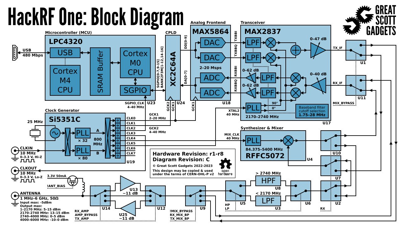
Three chips do the digital work:
- The NXP LPC4320FBD144 — a dual-core ARM Cortex-M4F + Cortex-M0 microcontroller. It runs the firmware, drives USB, and orchestrates everything else.
- The Xilinx CoolRunner-II XC2C64A — a 64-macrocell CPLD that implements the parallel-to-serial sample-shifting glue between the MAX5864 and the LPC4320’s SGPIO peripheral.
- The SiLabs Si5351C (Si5351A on r9) — a clock generator that derives every clock in the device from the 25 MHz crystal reference.
The digital subsystem differs in three places between revisions: r9 changed the Si5351C → Si5351A and added clock-distribution components; r10 reverted that. Otherwise the digital subsystem has been stable since r1.
3.2 The LPC4320
The LPC4320FBD144^[NXP product page: https://www.nxp.com/products/microcontrollers-and-processors/arm-processors/lpc-arm-cortex-m-mcus/lpc-dual-core-cortex-m0-m4f/lpc4300:MC_1403790133078. User manual: http://www.nxp.com/documents/user_manual/UM10503.pdf. Datasheet: http://www.nxp.com/documents/data_sheet/LPC4350_30_20_10.pdf.] is the brain. Key specs:
Table 1 — The LPC4320FBD144^[NXP product page: https://www.nxp.com/products/microcontrollers-and-processors/arm-processors/lpc-arm-cortex-m-mcus/lpc-dual-core-cortex-m0-m4f/lpc4300:MC1403790133078. User manual: http://www.nxp.com/documents/usermanual/UM10503.pdf. Datasheet: http://www.nxp.com/documents/datasheet/LPC4350302010.pdf.] is the brain. Key specs
| Parameter | LPC4320FBD144 |
|---|---|
| Cortex-M4F core | 204 MHz, single-precision FPU, DSP extensions |
| Cortex-M0 core | 204 MHz, asymmetric, runs in parallel |
| Internal SRAM | 200 KB (split across multiple banks) |
| External flash | None on-die; uses W25Q80BV SPIFI (8 Mbit) |
| USB 2.0 HS PHY | On-die, with on-die regulator |
| SGPIO peripheral | 16-bit, multi-mode parallel/serial shifter |
| GPIO pins | 144 in TQFP package (~80 usable) |
| Package | LQFP144 (20×20 mm) |
The LPC43xx family is unusual in being asymmetric multi-core — the M4F and the M0 share memory and bus fabric but run independent firmware images. On the HackRF, the M4F runs almost everything; the M0 is used by stock GSG firmware as a streaming co-processor that babysits the SGPIO peripheral while the M4F handles USB, SPI register writes to MAX2837/RFFC5072/Si5351C, and command handling.
The split is what makes 20 MS/s sustainable on a single-USB-endpoint design — the M4F could not both service USB and shovel samples through SGPIO at line rate; the M0 takes the sample-shovelling job.
3.2.1 The boot story
On power-up:
- The LPC4320 boots from internal ROM into a first-stage bootloader at the address selected by strapping pins. The HackRF straps boot from SPIFI (the W25Q80BV).
- ROM reads the SPIFI flash header; if a valid image is present, jumps to it.
- The HackRF firmware initialises clocks (via Si5351C SPI commands), brings up USB, configures GPIO direction registers, programs the CPLD bitstream if not already loaded, and lights up the front-panel LEDs.
- M0 firmware is started by the M4F as part of its init.
If the SPIFI flash is corrupt, the ROM falls back to DFU mode — enumerates as USB VID:PID 1d50:6088 and accepts a firmware image via the standard USB DFU protocol. This is the recovery path for “bricked” units; Vol 4 §3 walks the workflow.
3.3 The CPLD — Xilinx CoolRunner-II XC2C64A
The MAX5864’s parallel ADC/DAC interface is not directly compatible with the LPC4320’s SGPIO peripheral. The CPLD bridges the two:
- On the MAX5864 side: 8 data lines per direction (8-bit samples I or Q), a clock, and direction control.
- On the LPC4320 SGPIO side: a multi-bit shift register clocked from the same source, but with a different timing relationship.
The CPLD’s bitstream — a few KB of .xsvf data — implements a small state machine that reformats the parallel ADC bytes into the SGPIO’s expected serial-with-frame format. The bitstream lives in the firmware repo at firmware/cpld/sgpio_if/default.xsvf and is reflashed via:
hackrf_cpldjtag -x firmware/cpld/sgpio_if/default.xsvfAfter a successful flash, three LEDs on the board blink in a known pattern as the CPLD restarts. This step is not required for routine firmware updates — hackrf_spiflash updates the LPC4320 firmware only. The CPLD bitstream changes very rarely (handful of times in the project’s history).
The XC2C64A is a 64-macrocell device — small, cheap (~$3 in qty), and EEPROM-backed (retains its configuration across power cycles). Xilinx discontinued the CoolRunner-II family in 2022 but parts remain available and AMD/Xilinx promised long-term support in the discontinuation notice^[The CoolRunner-II discontinuation notice (XCN22020) is at https://www.amd.com/en/support/documentation-archive.html — search for “CoolRunner”. Long-term support runs through 2032 per Xilinx’s commitment.].
The HackRF Pro replaces the CPLD with a Lattice iCE40 UltraPlus FPGA (UP5K), which has roughly 5,000 LUTs vs the CoolRunner-II’s effective ~64 macrocells. The 80× capacity headroom is what enables the Pro’s planned digital-correction and extended-precision modes (Vol 4 §10).
3.4 The SGPIO Peripheral
The LPC4320’s SGPIO (Serial GPIO) peripheral is the single most important block on the chip from the HackRF’s perspective. SGPIO provides 16 32-bit shift registers that can be daisy-chained, gated by an external clock, and run independently of the CPU — essentially a small built-in DMA engine for parallel-to-serial conversion^[The SGPIO chapter in NXP’s UM10503 user manual covers this in detail: http://www.nxp.com/documents/user_manual/UM10503.pdf — Chapter 22.].
On the HackRF, SGPIO is configured to:
- Accept 8-bit parallel samples from the CPLD on a sample clock.
- Shift them into a 32-bit register that fills 4 samples deep.
- DMA the filled register to a system memory buffer.
- Generate an interrupt to the M0 when buffers are full or empty.
The M0 firmware is essentially a ring-buffer manager — it cycles through ~8 ring buffers in SRAM, marking them ready as SGPIO fills them, while the M4F copies them to USB endpoints. With 20 MS/s × 2 channels × 8 bits = 320 Mbit/s = 40 MB/s of sample data, this pipeline runs near the limit of what USB 2.0 high-speed (480 Mbit/s nominal, ~280 Mbit/s practical) can sustain. The HackRF firmware is tuned tight here — minor changes to ring-buffer sizes or interrupt service times can cause sample drops, which is why the firmware is conservative about feature additions to the streaming path.
GSG’s LPC43XX_SGPIO_Configuration.html in the docs^[https://hackrf.readthedocs.io/en/latest/LPC43XX_SGPIO_Configuration.html] is the authoritative reference for the SGPIO register settings used by the HackRF.
3.5 Clocking
There is one reference oscillator in the entire device: a 25 MHz quartz crystal (Y1 in the schematic) driving the Si5351C’s primary input.
The Si5351C^[https://www.silabs.com/timing/clocks/general-purpose-i2c-programmable-clocks/device.si5351c — the C-variant has 8 outputs and an additional CMOS input for clock disciplining; A-variant has 3 outputs and is used on r9 with extra board-level distribution to feed the same clock count.] is a clock-generator IC that takes one input frequency and produces up to 8 independently-programmable output frequencies via a fractional-N PLL + multi-synthesiser architecture. Programming is over I²C from the LPC4320.
The HackRF uses the Si5351C to generate:
Table 2 — The HackRF uses the Si5351C to generate
| Output | Frequency | Destination |
|---|---|---|
| CLK0 | Programmable (sample clock) | MAX5864 ADC/DAC clock |
| CLK1 | Programmable | RFFC5072 reference |
| CLK2 | 12 MHz | LPC4320 main clock (multiplied internally to 204 MHz) |
| CLK3 | Programmable | MAX2837 reference |
| CLK4–7 | Reserved | Spare; available for future use |
The MAX5864’s sample clock is set by the firmware as a function of the user’s requested sample rate — at 20 MS/s, CLK0 runs at 20 MHz; at lower rates, CLK0 runs at the matching rate.
3.5.1 The external CLKIN port
The HackRF One has a CLKIN port on the front panel — a U.FL or SMA (depending on rev) connector for an external 10 MHz reference. When activated by hackrf_clock --set-input-source external, the Si5351C is reprogrammed to lock its internal PLL to the external 10 MHz instead of the on-board 25 MHz crystal.
This is how you give a HackRF One absolute-frequency stability — feed it from a GPSDO, a rubidium reference, or a lab signal generator. The Si5351C’s PLL bandwidth is ~10 kHz, so the external reference’s phase noise inside that bandwidth dominates; outside, the Si5351C’s noise floor takes over.
For two-HackRF synchronised work (TDOA, direction finding, IQ-coherent dual-receive), the canonical setup is:
[GPSDO 10 MHz] ── splitter ─┬─► HackRF #1 CLKIN
                            │
                            └─► HackRF #2 CLKIN
Vol 5 §7 walks the hackrf_clock CLI in detail.
3.5.2 Why this matters for absolute frequency
A 25 MHz crystal at room temperature has a tolerance of ±20 ppm over its operating range. At 2.4 GHz tuning, ±20 ppm is ±48 kHz of frequency uncertainty — enormous for narrowband digital modes (FT8 at ±2 Hz, WSPR at ±1 Hz, even FM voice at ±5 kHz). Drift over a 30-minute warm-up is typically half this — but it’s still ±24 kHz on a cold device.
Solutions in increasing order of cost:
- Warm-up + manual offset — let the device sit powered for 30 minutes, measure the offset against a known reference, set
--ppm-offsetin receiver software. Acceptable for casual work above 100 MHz. - External GPSDO into CLKIN — $80–250 part. Brings stability to <1 ppb. Vol 5 §7 covers wiring and software setup.
- Buy the HackRF Pro — built-in TCXO replaces the crystal. Sub-ppm without external hardware.
3.6 The USB Stack
USB 2.0 high-speed (480 Mbit/s nominal) is the host interface. The LPC4320’s on-die USB PHY drives a single USB endpoint pair: bulk IN (samples to host) and bulk OUT (samples from host) on the streaming path, plus control endpoints for the command surface.
The vendor-specific HackRF USB protocol is documented in hackrf-tools/host/hackrf-tools/src/hackrf.h of the host repo and consists of about 60 vendor commands^[https://github.com/greatscottgadgets/hackrf/blob/main/host/libhackrf/src/hackrf.h]:
Table 3 — The vendor-specific HackRF USB protocol is documented in hackrf-tools/host/hackrf-tools/src/hackrf.h of the host repo and consists of about 60 vendor commands^[https://github.com/greatscottgadgets/hackrf/blob/main/host/libhackrf/src/hackrf.h]
| Command class | Examples |
|---|---|
| Identification | BOARD_ID_READ, VERSION_STRING_READ, SERIAL_READ |
| Sample rate | SET_SAMPLE_RATE |
| Frequency | SET_FREQUENCY, SET_FREQUENCY_EXPLICIT |
| Gain | SET_LNA_GAIN, SET_VGA_GAIN, SET_TXVGA_GAIN |
| TX/RX mode | SET_TRANSCEIVER_MODE |
| Streaming | START_RX, START_TX, STOP |
| Bias-T | SET_ANTENNA_ENABLE |
| Clock | GET_CLKIN_STATUS, SET_CLKOUT_ENABLE |
| Sweep | INIT_SWEEP |
| Firmware | SPIFLASH_READ, SPIFLASH_WRITE, RESET |
libhackrf wraps these into a friendly C API; libhackrf is what hackrf_transfer, hackrf_sweep, and every host application uses (Vol 5).
USB enumeration as device VID:PID 1d50:6089 in normal mode, 1d50:6088 in DFU mode. The vendor ID 1d50 is “OpenMoko, Inc.” and is shared with several open-hardware projects.
3.7 GPIO Allocation
Of the 144 LPC4320 pins, the HackRF uses approximately:
Table 4 — Of the 144 LPC4320 pins, the HackRF uses approximately
| Group | Pins | Purpose |
|---|---|---|
| SGPIO 0–7 (sample data) | 8 | Parallel sample data to/from CPLD |
| SGPIO clock/sync | 4 | Sample clock + frame strobe + control |
| SPI to MAX2837 | 4 | Register writes; MAX2837 doesn’t use SPI for data |
| SPI to RFFC5072 | 4 | LO programming |
| I²C to Si5351C | 2 | Clock generator config |
| RF switch control | 2–4 | SP4T path select (decoded vs encoded — depends on switch part) |
| Bias-T enable | 2 | Per-direction enable (RX, TX) |
| LEDs | 3 | USB / RX / TX activity |
| User button | 1 | DFU mode entry |
| Reserved expansion header | 32 | The PortaPack uses many of these |
| Hardware revision strap pins (r6+) | 3 | Self-reported revision |
| USB | 4 | DP, DM, VBUS, GND |
The expansion header (P22 on the schematic) is what the PortaPack mates to. Vol 9 §3 covers the pinout in full.
3.8 Memory Map
The LPC4320’s address space:
Table 5 — The LPC4320's address space
| Range | Region |
|---|---|
| 0x00000000 – 0x000FFFFF | Internal Boot ROM (factory programmed, read-only) |
| 0x10000000 – 0x10007FFF | Local SRAM bank 0 (32 KB) — M4F-favoured |
| 0x10080000 – 0x1009FFFF | Local SRAM bank 1 (40 KB) |
| 0x14000000 – 0x14FFFFFF | SPIFI external flash window (W25Q80BV mapped here) |
| 0x20000000 – 0x20007FFF | AHB SRAM bank 0 (32 KB) — typically M0-favoured |
| 0x20008000 – 0x2000BFFF | AHB SRAM bank 1 (16 KB) — sample ring buffers |
| 0x40000000 – 0x4FFFFFFF | Peripheral registers (USB, SGPIO, SPI, I²C, GPIO, etc.) |
The sample ring buffers live in AHB SRAM — accessible by both cores and by the SGPIO DMA engine without contention with the M4F’s instruction fetches.
3.9 Interrupt Architecture
The streaming path runs in interrupt context. The hot path:
- SGPIO DMA fills a ring-buffer slot.
- SGPIO interrupt fires → M0 ISR marks the slot ready.
- M4F’s USB ISR fires when USB endpoint is ready for more data.
- USB ISR reads the next ready slot from M0’s ring, DMAs it to USB, marks the slot free.
- SGPIO sees the free slot, fills it, repeat.
This pipeline runs at 40 MB/s without dropping samples on a clean USB chain. The conditions that cause drops:
- Host buffering issues — laptop with slow USB host controller, or competing USB devices on the same root hub. Solution: dedicated USB chain.
- CPU load on the host — the host application can’t drain the USB pipe fast enough. Solution: drop sample rate, or run the capture on a more powerful machine.
- Power dips — the HackRF draws ~500 mA on USB 2.0 (full spec), and a marginal cable or hub causes voltage sag that triggers unexpected resets.
hackrf_transfer reports drops in its end-of-run summary; if the count is > 0, the data has gaps.
3.10 The CPLD Recovery Path
Occasionally — usually after a botched firmware development experiment, never in routine use — the CPLD bitstream becomes corrupt. Symptoms: hackrf_info works (LPC4320 firmware is fine) but no samples flow.
Recovery:
# 1. Confirm the LPC firmware is alive
$ hackrf_info
# Should show device + firmware version. If this fails, see Vol 4 §3
# (DFU recovery — different problem).

# 2. Reflash the CPLD bitstream (default-known-good)
$ git clone https://github.com/greatscottgadgets/hackrf
$ cd hackrf
$ hackrf_cpldjtag -x firmware/cpld/sgpio_if/default.xsvf

# 3. Wait for the LEDs to blink (3-5 seconds), then reset
$ hackrf_transfer -r /dev/null -f 100000000 -s 2000000 -n 1000000
# Should succeed without "samples not received" errors
This procedure is in hackrf_cpldjtag.c of the host tools and on the GSG troubleshooting page^[https://hackrf.readthedocs.io/en/latest/troubleshooting.html].
3.11 Differences in the HackRF Pro
The HackRF Pro’s digital subsystem replaces:
- CPLD → iCE40 UltraPlus FPGA (UP5K) — 5280 LUTs, BRAM blocks, DSP slices. Open-source toolchain via Yosys + nextpnr-ice40.
- Flash → W25Q32 (32 Mbit, 4× the One). Holds a larger firmware image and FPGA bitstream.
- MCU → still LPC4320 (planned upgrade in a future revision).
The FPGA capacity headroom enables features the CPLD couldn’t fit:
- Digital pre-distortion of the TX path (compensates for mixer non-linearity).
- Extended-precision sample modes (12-bit equivalent via oversampling + decimation).
- Built-in test signal generator at the FPGA fabric level.
- Future modes that the firmware team has not yet announced.
The Pro’s iCE40 is JTAG-flashed by the firmware on every boot — there is no separate hackrf_cpldjtag step for the Pro. The bitstream lives in the firmware image and is loaded into the FPGA by the LPC4320 over a dedicated SPI link at startup.
3.12 Cheatsheet Updates from this Volume
For Vol 12:
- LPC4320 dual-core: M4F + M0; M0 babysits SGPIO
- USB streaming: 40 MB/s sustained, 20 MS/s × 2 channels × 8-bit
- Si5351C: I²C-programmable, 8 outputs, locked to 25 MHz crystal or external 10 MHz CLKIN
- CPLD recovery:
hackrf_cpldjtag -x firmware/cpld/sgpio_if/default.xsvf - DFU mode entry: hold DFU button while plugging USB → enumerates as 1d50:6088
- Memory map: AHB SRAM 0x20000000–0x2000BFFF for ring buffers
- HackRF Pro: iCE40 UP5K FPGA replaces CPLD; 4× more flash
3.13 Resources
Table 6 — 13. Resources
Comments (0)